Description
We provide the world's largest size commercially available GaS crystals at the highest quality GaS and affordable prices. Our crystals exceed competing crystals both in size and quality.
Description
Large-size hexagonal phase GaS (Gallium sulfide) crystals have been developed at our facilities using three different growth techniques: Bridgman growth, chemical vapor transport (CVT), and flux zone growth. These techniques have been optimized to achieve grain sizes and reduce defect concentrations. In contrast to the commonly used chemical vapor transport (CVT) technique, flux grown crystals are well known for their structural perfection and electronic/optical performance. Bridgman and flux zone methods both offer similar grade qualities. Each crystal is very large in size to last for years, is highly crystalline, oriented in 0001 direction, and easy to exfoliate. Our R&D staff takes a characterization dataset in each sample piece to ensure structural, optical, and electronic consistency.Properties of monoclinic GaS vdW crystals
| Crystal size | > 1 cm in size and perfectly 0001 oriented |
| Material properties | 2.55 eV indirect semiconductor (bulk) |
| Crystal structure | Hexagonal phase |
| Unit cell parameters | a=0.360, b=0.640 nm, c=1.544 nm, α=β=90°, γ=120° |
| Growth method | Bridgman Growth [Optional CVT or Flux zone growth also available] |
| Purity | Better than 99.9999% confirmed |
Growth method matters> Flux zone or CVT growth method? Contamination of halides and point defects in layered crystals are well known cause for their reduced electronic mobility, reduced anisotropic response, poor e-h recombination, low-PL emission, and lower optical absorption. Flux zone technique is a halide free technique used for synthesizing truly semiconductor grade vdW crystals. This method distinguishes itself from chemical vapor transport (CVT) technique in the following regard: CVT is a quick (~2 weeks) growth method but exhibits poor crystalline quality and the defect concentration reaches to 1E11 to 1E12 cm-2 range. In contrast, flux method takes long (~3 months) growth time, but ensures slow crystallization for perfect atomic structuring, and impurity free crystal growth with defect concentration as low as 1E9 - 1E10 cm-2. During check out just state which type of growth process is preferred. Unless otherwise stated, 2Dsemiconductors ships Flux zone crystals as a default choice.
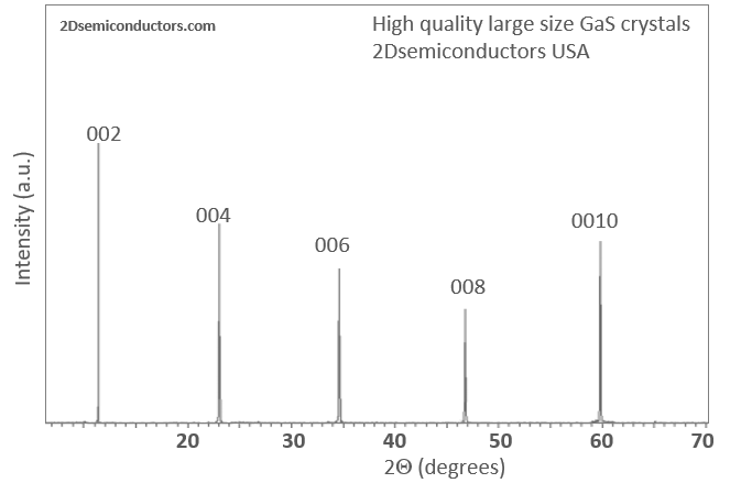
XRD data collected from vdW GaS crystals

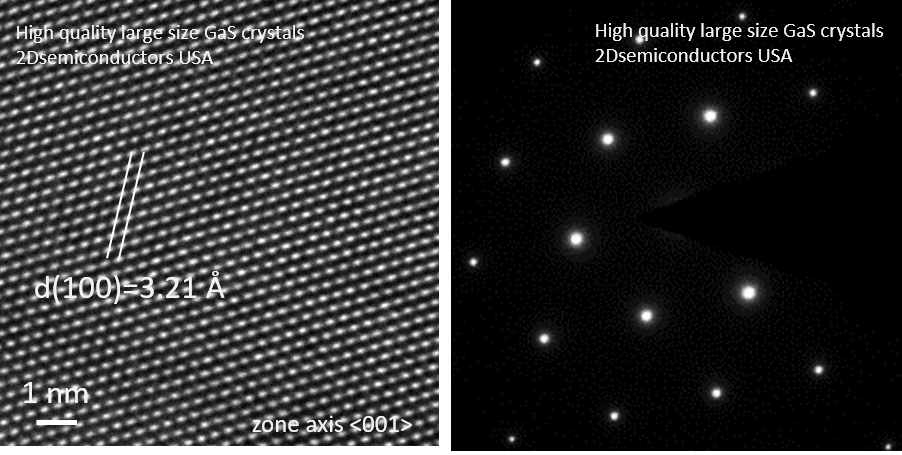
HRTEM and SAED characterization on GaS vdW crystals by 2Dsemiconductors USA

Raman spectrum collected from vdW GaS crystals

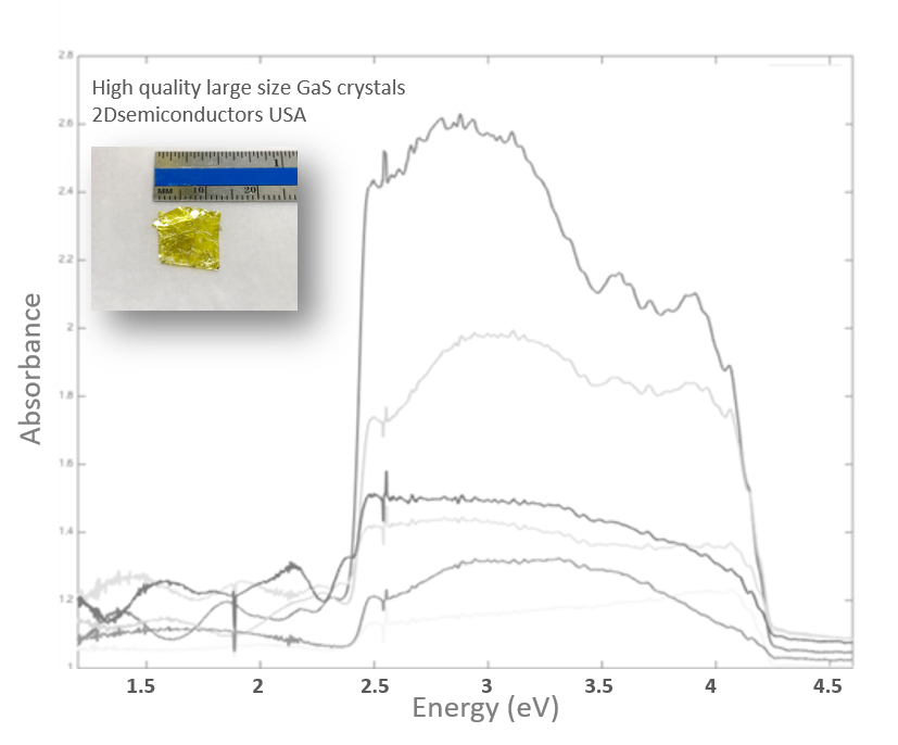
Absorbance spectrum collected from GaS vdW crystals

Additional Information
Elements: |
Ga,S |
Element: |
Gallium |
Element: |
Sulfur |
Formula: |
GaS |
Material class: |
MX |
Properties: |
Semiconductor |
Band gap range: |
VIS |
Growth method: |
Bridgman |
Growth method: |
Flux |
Growth method: |
CVT |
Doping: |
Undoped |


