Our Story
2Dsemiconductors Inc. Pioneering the Path from Discovery to Disruption

Our vision.
At 2Dsemiconductors, our vision is to make these niche materials accessible to all, academia, startups, and industry alike. We strive to democratize innovation by offering novel material systems and state-of-the-art synthesis methods at a fraction of the traditional cost, without compromising on quality or precision. We strive to enable groundbreaking research and commercialization, not just for a select few, but for the entire innovation community. True progress, we believe, happens when knowledge is shared, barriers are removed, and exploration is within reach for all.
At 2Dsemiconductors, our vision has always been clear: to close the gap between academic discovery and industrial application, and to drive materials science forward by doing what others won’t: taking bold risks, innovating new material systems, and pushing the boundaries of what’s scientifically and technologically possible. We are motivated by the belief that true progress in semiconductors, quantum materials, and next-generation systems happens at the edge of exploration, not within the confines of conventional practice.
From Foundation to Global Impact. We began as a small, research-driven initiative led by engineers with deep roots in research, process engineering, and technology design. Our first major expansion came in 2014, allowing us to scale operations and expand our offerings. In 2018, we launched a second expansion, this time dramatically increasing our infrastructure, processing capabilities, and lab space to meet growing international demand. In 2023, we completed a third expansion, further solidifying our capacity for rapid development and delivery of novel materials.
Today, we are actively planning our next wave of global growth with future sites in Germany (EU), India, and Japan, designed to accelerate innovation pipelines and strengthen regional collaboration with global research hubs and advanced manufacturing centers.
Innovation. Innovation is the heartbeat of our company. Since inception, we’ve introduced over 500 quantum and emergent material systems, world record in this domain, at a rate unmatched in the field. Our materials power discovery across electronics, optoelectronics, quantum devices, chemistry, biology, and more. With advanced growth techniques, we continue to lead the charge in exploring and commercializing materials once considered out of reach.
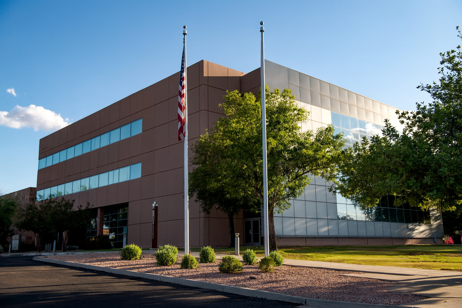
Strategic Location. Our headquarters in Phoenix places us at the epicenter of the U.S. semiconductor ecosystem, with immediate proximity to global industry leaders including TSMC, Intel, Samsung, Applied Materials, Infineon, Honeywell, ON semiconductors, Raytheon, and several cutting-edge GaN and advanced packaging companies. This strategic location enables rapid collaboration, streamlined logistics, and direct access to a deep and diverse talent pool, fueling innovation and accelerating impact across the semiconductor value chain.
Clientele. With over 10,000 clients worldwide, including Fortune 500 companies, national laboratories, research universities, mid-sized innovators, and emerging startups, we have built a reputation for reliability, technical leadership, and speed. Our materials and services are trusted across disciplines and industries, helping scientists and engineers bring their boldest ideas to life.
Approach. What sets us apart is our willingness to take risks and enter scientific territory where others hesitate. At 2Dsemiconductors, exploration and experimentation are core to our DNA. Whether we’re developing a new material system, scaling up a novel growth process, or collaborating with global partners, our fearless approach ensures we stay ahead of what’s next.
As we celebrate our first decade, we reflect on a journey shaped by innovation, collaboration, and a relentless pursuit of excellence. Our legacy is not only defined by the materials we’ve delivered, but by the future we’re helping to build. With eyes on the next frontier, 2Dsemiconductors is poised for another decade of global impact, continuing to redefine what’s possible in science and engineering.
Cost Statement: The True Value Behind Every Crystal
Producing advanced materials at the frontier of science is no small feat. It requires deep expertise, specialized infrastructure, and a multidisciplinary team working together across research, operations, and customer support. Behind every crystal is a network of highly skilled professionals, including materials scientists, engineers, legal advisors, accountants, designers, web developers, photographers, customer service and logistics staff, front-line sales, and media and communications specialists. Each layer of this operation, from precise synthesis to global delivery, contributes to the overall cost of creating and supplying these materials.
Maintaining high-quality production also involves significant investments in research and development, expensive precursors, equipment acquisition and maintenance, facility rentals, building upkeep, R&D expenses, and continuous innovation. We proudly operate with full transparency and contribute nearly 40 percent of all sales as taxes, supporting the broader economy and innovation ecosystem.
Despite these real and rising costs, we are committed to keeping our prices accessible. Our goal is to ensure that world-class materials are within reach for academic researchers, startups, and industrial users at all stages of development.
In fact, producing these materials within academic settings often requires even more resources. Postdoc salaries, Ph.D. student tuition, materials and supplies, equipment depreciation, equipment upkeep, facility overhead, infrastructure, and metrology all add up quickly. Institutional overhead rates further increase costs, often making in-house synthesis significantly more expensive, less productive (crystal yield), and time consuming.
By centralizing expertise, optimizing production, and operating at scale, 2Dsemiconductors reduces barriers to access. We make it possible for a wider community of innovators to obtain and explore the materials that define the future of science and technology.
