Description
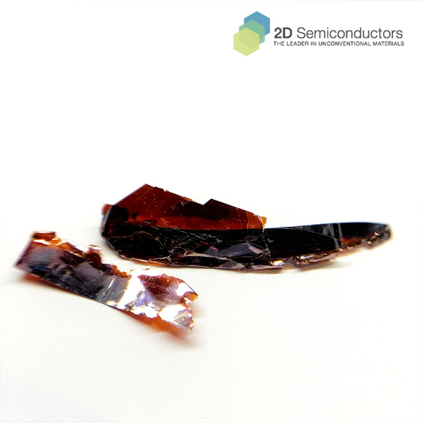
Our HfS2 crystals are grown using ultra pure flux vapor technique to produce crystal that are free of halides and vacancy defects. The defect concentration remains lower than 1E9cm-2 for high optical and electronic performance. Our growth technique has been designed and optimized since 2011 to achieve perfect industrial semiconductor grade materials with: 1) excellent stoichiometry, 2) large single domain size, 3) single phase materials without any mixed phases or amorphous content, 4) perfect layered crystal ideal for exfoliation purposes with impressive mosaic spread 0.08 degrees, 5) unmatched purity -semiconductor grade (6N), 99.9999%.
The properties of HfS2 crystals
Hafnium disulfide (HfS₂) is an indirect gap layered semiconductor in the bulk and becomes direct gap semiconductor in monolayer form.
| Dopants | Undoped (intrinsic semiconductor) |
| Material properties | ~2eV indirect gap semiconductor |
| Crystal structure | Hexagonal phase |
| Unit cell parameters | a=b=0.362 nm, c=0.580 nm; α=β=90°, γ=120° |
| Growth method | [Default] Flux zone (no halide contamination) defect free [Optional CVT]: Contains Br2, Cl2, TeCl4, and other halides |
| Purity | 99.9999 confirmed |
Growth method matters> Flux zone or CVT growth method? Contamination of halides and point defects in layered crystals are well known cause for their reduced electronic mobility, reduced anisotropic response, poor e-h recombination, low-PL emission, and lower optical absorption. Flux zone technique is a halide free technique used for synthesizing truly semiconductor grade vdW crystals. This method distinguishes itself from chemical vapor transport (CVT) technique in the following regard: CVT is a quick (~2 weeks) growth method but exhibits poor crystalline quality and the defect concentration reaches to 1E11 to 1E12 cm-2 range. In contrast, flux method takes long (~3 months) growth time, but ensures slow crystallization for perfect atomic structuring, and impurity free crystal growth with defect concentration as low as 1E9 - 1E10 cm-2. During check out just state which type of growth process is preferred. Unless otherwise stated, 2Dsemiconductors ships Flux zone crystals as a default choice.
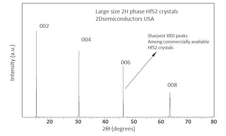
XRD data collected from HfS2 crystals

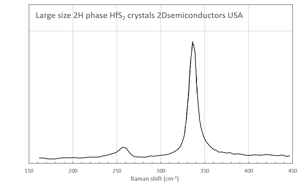
Raman spectrum collected from HfS2 crystals

Example recent work citing our products
"High oscillator strength interlayer excitons in two-dimensional heterostructures for mid-infrared photodetection"
Nature Nanotechnology volume 15, pages675–682 (2020)
"Dynamically reconfigurable electronic and phononic properties in intercalated HfS2"
Materials Today, 39, 110 (2020)
"Chemical bonding and Born charge in 1T-HfS2"
Nature 2D Materials and Applications volume 5, Article number: 45 (2021)
Additional Information
Elements: |
Hf,S |
Element: |
Hafnium |
Element: |
Sulfur |
Formula: |
HfS2 |
Material class: |
MX2 |
Material class: |
Dichalcogen |
Properties: |
Semiconductor |
Properties: |
Excitonic |
Band gap range: |
VIS |
Growth method: |
Flux |
Growth method: |
CVT |
Doping: |
Undoped |


