Description
Layered tellurene crystals have been synthesized in through hydrothermal synthesis method to provide an easier way to yield thin tellurene sheets. Unlike bulk tellurene materials, hyrothermally synthesized Tellurene are in thin ribbon shapes and are slightly easier to exfoliate. Layered tellurium (Te) has a trigonal crystal lattice (see product images) in which individual helical chains of Te atoms are stacked together by van der Waals type bonds and spiral around axes parallel to the [0001] direction at the center and corners of the hexagonal elementary cell [1-2]. Tellurene exhibits a tunable bandgap varying from nearly direct 0.31 eV (bulk) to indirect 1.17 eV (2L) and direct at 1.3 eV (1L) [3]. It has been shown to exhibit metallic behavior under certain conditions and even host DCWs. It has four (two) complex, highly anisotropic and layer-dependent hole (electron) pockets in the first Brillouin zone with an extraordinarily high hole mobility reaching up to theoretical ∼1E5 cm2/Vs value [1-3].
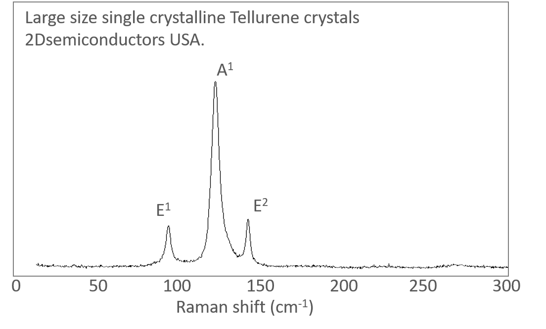
Raman spectrum collected from Tellurene crystals under 532 nm laser excitation

XRD data collected from tellurene crystals

Related references
[1] "Two-dimensional tellurium" Nature 552, 40-41 (2017) [Page link]
[2] "Large-area solution-grown 2D tellurene for air-stable, high-performance field-effect transistors"; arXiv:1704.06202 [Page link]
[3] "Few-layer Tellurium: one-dimensional-like layered elementary semiconductor with striking physical properties" ; https://doi.org/10.1016/j.scib.2018.01.010 [Page link]
Additional Information
Elements: |
Te |
Element: |
Tellurium |
Formula: |
Te |
Material class: |
Element |
Material class: |
Quasi-1D |
Properties: |
Semiconductor |
Properties: |
High mobility |
Band gap range: |
IR |
Growth method: |
Hydrothermal synthesis |
Doping: |
Undoped |


