Description
Our single crystal ReS₂ (Rhenium disulfide) crystals are produced in world-record sizes exceeding 1 cm, setting a new benchmark in the field. These crystals are meticulously grown in our facilities using optimized chemical vapor transport and flux zone techniques, refined over 9 years to achieve superior anisotropic properties. The ReS₂ crystals exhibit remarkable structural anisotropy from bulk to monolayer, verified by comprehensive analyses including XRD, TEM, angle-resolved Raman spectroscopy, and photoluminescence measurements.
Typical characteristics of ReS2 crystals from 2Dsemiconductors
| Crystal size | + 1 cm in size |
| Dopants | intrinsic semiconductor (for doping, please contact us) |
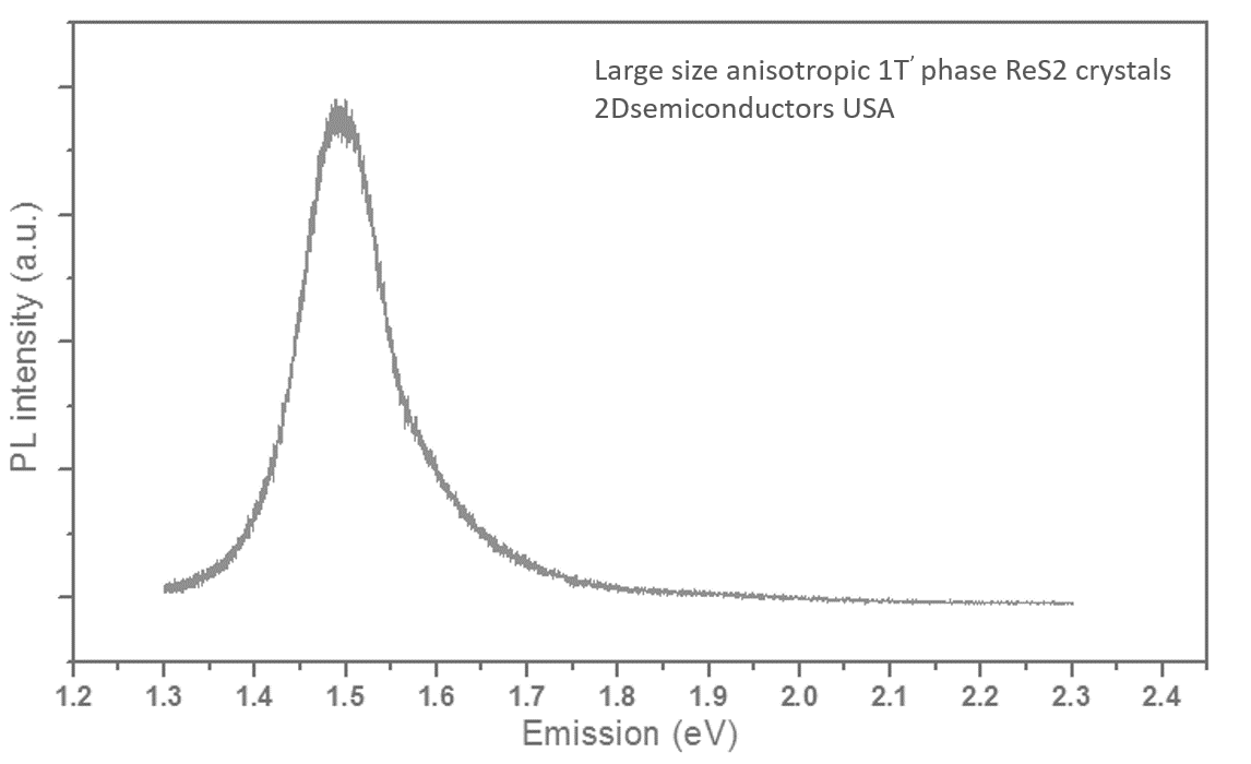
| Material properties | ~1.4 eV emission (300K), direct/indirect gap semiconductor |
| Crystal structure | 1T' phase (anisotropic semiconductor) |
| Unit cell parameters | a=0.633 nm, b=0.638 nm, c=0.665 nm; α=106.7°, β=119°, γ=89.98° |
| Growth method | [Default] Flux zone (no halide contamination) defect free [Optional CVT]: Contains Br2, Cl2, TeCl4, and other halides |
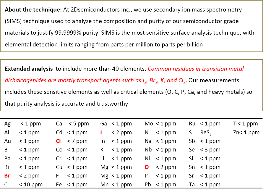
| Purity |
99.9999% confirmed
|
Growth method matters> Flux zone or CVT growth method? Contamination of halides and point defects in layered crystals are well known cause for their reduced electronic mobility, reduced anisotropic response, poor e-h recombination, low-PL emission, and lower optical absorption. Flux zone technique is a halide free technique used for synthesizing truly semiconductor grade vdW crystals. This method distinguishes itself from chemical vapor transport (CVT) technique in the following regard: CVT is a quick (~2 weeks) growth method but exhibits poor crystalline quality and the defect concentration reaches to 1E11 to 1E12 cm-2 range. In contrast, flux method takes long (~3 months) growth time, but ensures slow crystallization for perfect atomic structuring, and impurity free crystal growth with defect concentration as low as 1E9 - 1E10 cm-2. During check out just state which type of growth process is preferred. Unless otherwise stated, 2Dsemiconductors ships Flux zone crystals as a default choice.
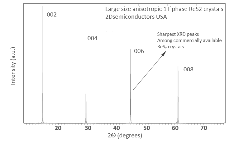
XRD data collected from ReS2 crystals

Raman spectrum collected from ReS2 monolayers

PL spectrum collected from ReS2 on SiO2/Si substrates

SIMS purity datasets collected from ReS2 crystals

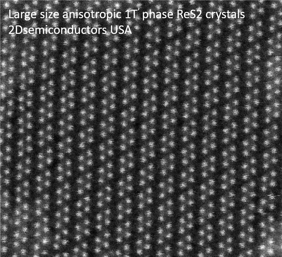
HRTEM images collected from ReS2 crystals

"High Responsivity Phototransistors Based on Few-Layer ReS2 for Weak Signal Detection"
Advanced Functional Materials https://doi.org/10.1002/adfm.201504408
D. Wolverson et,al. "Rhenium Dichalcogenides: Layered Semiconductors with Two Vertical Orientations," Nano Letters 2016, 16, 1381−1386
Ignacio Gutiérrez-Lezama et. al. "Electroluminescence from indirect band gap semiconductor ReS2" 2D Materials, Volume 3, Number 4
Manish Chhowalla, "Two-dimensional semiconductors for transistors" Nature Reviews Materials 1, Article number: 16052 (2016) doi:10.1038/natrevmats.2016.52
Q. Cui et. al. "Coherent Control of Nanoscale Ballistic Currents in Transition Metal Dichalcogenide ReS2" ACS Nano 10.1021/acsnano.5b01111 (2015)
X-F. Qiao et.al. "Polytypism and unexpected strong interlayer coupling in two-dimensional layered ReS2" Nanoscale, 2016, 8, 8324 (2016)
D. Wolverson et.al. "Raman Spectra of Monolayer, Few-Layer, and Bulk ReSe2: An Anisotropic Layered Semiconductor" ACS Nano, 2014, 8 (11), pp 11154–11164
E. Lorchat et.al. "Splitting of Interlayer Shear Modes and Photon Energy Dependent Anisotropic Raman Response in N-Layer ReSe2 and ReS2" ACS Nano, 2016, 10 (2), pp 2752–2760
Additional Information
Elements: |
Re,S |
Element: |
Rhenium |
Element: |
Sulfur |
Formula: |
ReS2 |
Material class: |
MX2 |
Material class: |
Dichalcogen |
Material class: |
Quasi-1D |
Properties: |
Semiconductor |
Properties: |
Excitonic |
Band gap range: |
VIS |
Growth method: |
Flux |
Growth method: |
CVT |
Doping: |
Undoped |
Doping: |
p-Type |
Doping: |
n-Type |


