Description
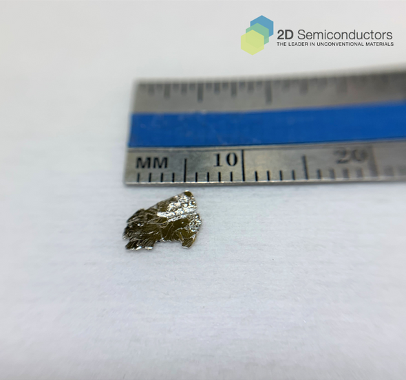
1T-phase TiSe2 crystals are vdW semimetals with charge density wave properties below Tc~202K. Our TiSe2 measure nearly 1 cm in size and are notoriously known low impurity resistance (zero temperature resistance), high carrier mobility, extremely clean and sharp XRD peaks, and negligible amount of defects. They are grown with solid state sciences application, electronic, and optical measurements in mind to reach scientific grade qualtiy and 99.9999% purity. These crystals are mainly grown by two different techniques, namely chemical vapor transport (CVT) and flux zone growth. The former method is commonly used in field for quick material growth but they exhibit large amount of halide contaminants and point defects. In contrast, flux method produces crystals in 3-4 months but excel at achiving high crystallinity and purity materials. Our flux zone grown TiSe2 crystals are treated as gold standards in 2D materials field owing to perfected electronic behavior with guaranteed CDW response. All crystals are perfectly layered and ready for exfoliation without any preparation. If you research needs STM grade surfaces please contact us, we will be happy to arrange these samples.
Properties of vdW TiSe2 crystals
| TiSe₂ | Metal, semimetal, CDW (~204K) |
| Crystal structure | CDW phase |
| Unit cell parameters | a=b=0.354 nm, c=0.601 nm; α=β=90° ,γ=120° |
| Growth method | Flux zone (guaranteed no halide contamination) [On request: chemical vapor transport (CVT) grown crystals may contain defects and halides contaminants] |
| Purity | 99.9999% confirmed |
Growth method matters> Flux zone or CVT growth method? Contamination of halides and point defects in layered crystals are well known cause for their reduced electronic mobility, reduced anisotropic response, poor e-h recombination, low-PL emission, and lower optical absorption. Flux zone technique is a halide free technique used for synthesizing truly semiconductor grade vdW crystals. This method distinguishes itself from chemical vapor transport (CVT) technique in the following regard: CVT is a quick (~2 weeks) growth method but exhibits poor crystalline quality and the defect concentration reaches to 1E11 to 1E12 cm-2 range. In contrast, flux method takes long (~3 months) growth time, but ensures slow crystallization for perfect atomic structuring, and impurity free crystal growth with defect concentration as low as 1E9 - 1E10 cm-2. During check out just state which type of growth process is preferred. Unless otherwise stated, 2Dsemiconductors ships Flux zone crystals as a default choice.
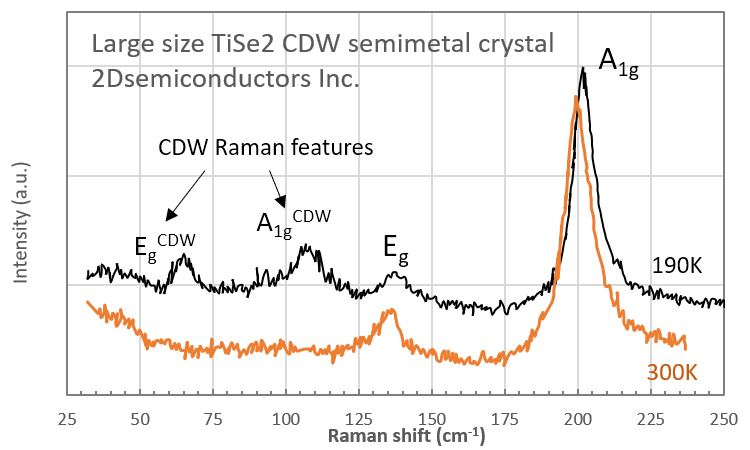
Raman spectrum collected from TiSe2 crystals above and below CDW transition temperature
Raman spectroscopy measurements performed by our R&D staff show progression of CDW Raman features when the temperature is lowered below CDW transition temperature
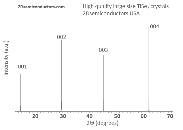
XRD data collected from vdW TiSe2 crystals
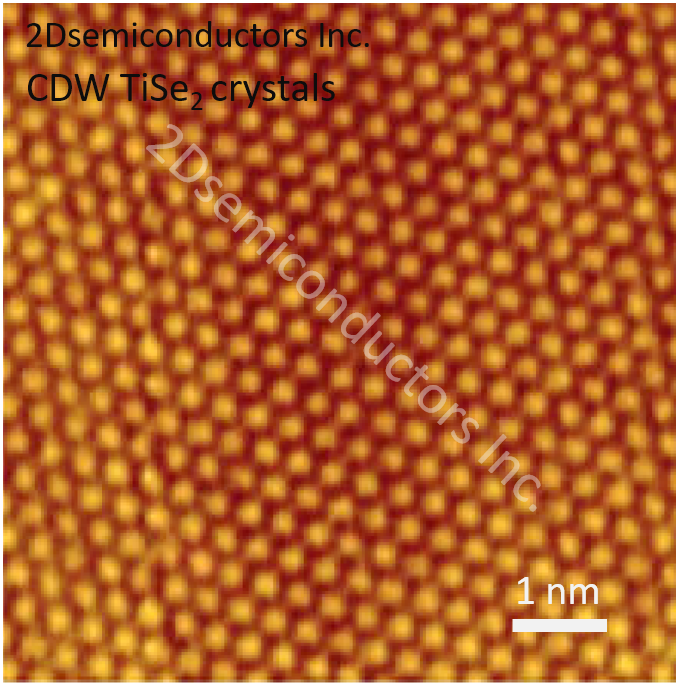
Scanning tunneling microscopy (STM) scans from TiSe2 crystals
Additional Information
Elements: |
Ti,Se |
Element: |
Titanium |
Element: |
Selenium |
Formula: |
TiSe2 |
Material class: |
MX2 |
Material class: |
Dichalcogen |
Properties: |
Semimetal |
Properties: |
CDW |
Growth method: |
CVT |
Doping: |
Undoped |


