Description
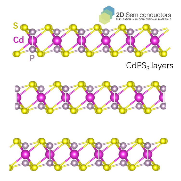
Unlike usual chemical vapor transport growth, these crystals has been synthesized using flux zone growth method to ensure no defects are present and no other phases (such as CdS2, CdS, PO2) are present. Crystals are 100% electronic, optical, and magnetic grade. If needed, our team can also electronically dope CdPS3 using Au, Pd, or Ag. CdPS3 is layered crystal that belongs to a large family of MPX3 where M is the divalent transition metal, P is phosphorus, and X is sulfur. It crystallizes in CdI2 type structure and at room temperature appears in the monoclinic C2/m phase. It exhibits an optical band gap ranging from 3.0 to 3.5 eV depending on various sources. It exhibits low temperature structural phases. While CdPS3 crystals have been synthesized their properties in the 2D limit still remains unknown.
The properties of CdPS3 crystals
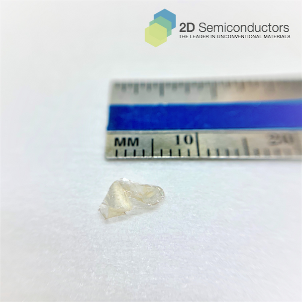
| Sample size | ~5 mm sized crystals |
| Material properties | Excitonic semiconductor, phase change materials |
| Crystal structure | Layered phase |
| Degree of exfoliation | Easy exfoliation characteristics |
| Production method | CVT technique [Optional: Flux growth ] |
| Other characteristics |
|
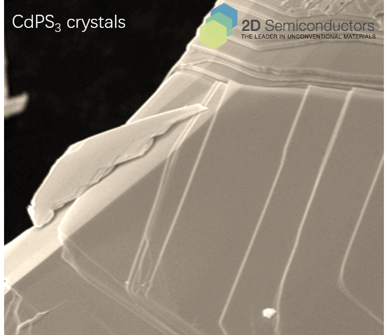
Layered nature of CdPS3 crystals from SEM images

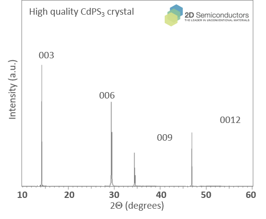
XRD data collected from CdPS3 crystals

Atomic structure of CdPS3

Reference
Acoustic phonons and elastic stiffnesses from Brillouin scattering of CdPS3
Journal of Applied Physics 131, 165109 (2022)
Additional Information
Elements: |
Cd,P,S |
Element: |
Cadmium |
Element: |
Phosphorus |
Element: |
Sulfur |
Formula: |
CdPS3 |
Material class: |
MPX3 |
Properties: |
Semiconductor |
Properties: |
Magnet |
Band gap range: |
VIS |
Growth method: |
CVT |
Growth method: |
Flux |
Doping: |
Undoped |


