Description
World's only Commercial High-Pressure Grown h-BN Crystals: The Gold Standard in 2D Materials
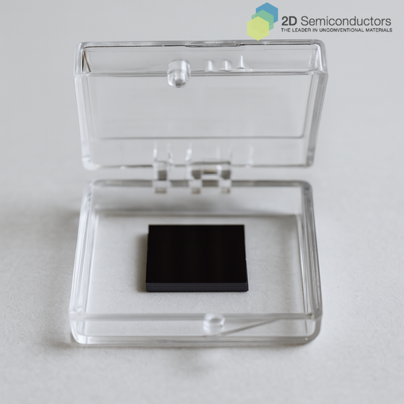
We offer the world's only high-pressure grown hexagonal boron nitride (h-BN) crystals, widely regarded as the gold standard in the 2D materials community. Each package includes 5 to 10 crystals, typically ranging from 0.5 mm to 1.5 mm in size.
We offer two techniques
1. High-Pressure h-BN Growth
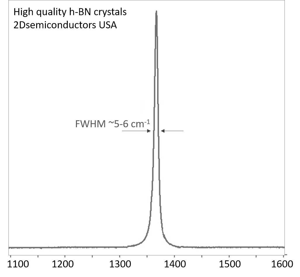
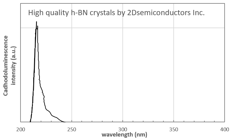
Our high-pressure method delivers the highest purity and lowest defect density h-BN crystals available commercially. These crystals have purity levels up to 99.9999 percent and defect concentrations as low as 1E8 to 1E10 cm-2. They feature sharp Raman peaks with full width at half maximum (FWHM) below 5.0 cm-1 and clear cathodoluminescence signals.
This process takes place at pressures above 10 GPa in a vacuum environment using a Ba/Be-BN solution growth method developed at our facility. The resulting crystals are free of surface oxides and ideal for high-performance electronic and photonic applications.
Each package contains 5 to 10 crystals between 0.5 mm and 1.5 mm in size.
2. Atmospheric Pressure h-BN Growth
This growth method produces high-quality h-BN crystals with slightly higher defect concentrations, typically around 1E9 to 1E10 cm-2. These crystals are slightly thicker and can reach up to 1.5 mm in lateral size, making them excellent for heterostructure and heterojunction fabrication.
The process occurs at atmospheric pressure using a specialized metal alloy solution to precipitate and grow h-BN. While these crystals may not exhibit clear cathodoluminescence, they are still electronic-grade and suitable for device integration.
All growth is performed at temperatures exceeding 1600 °C using advanced techniques including cubic anvil cells, boron nitride enclaves, and diamond press systems. Each package includes 5 to 10 crystals measuring 0.5 mm to 1.5 mm.
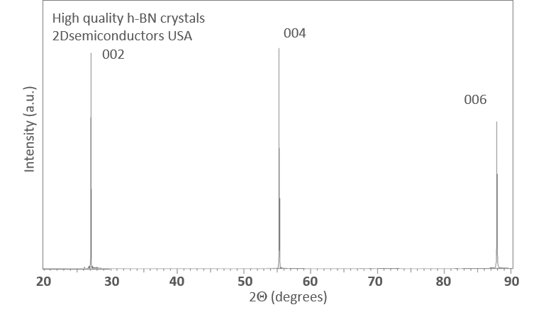
XRD data collected from h-BN crystals
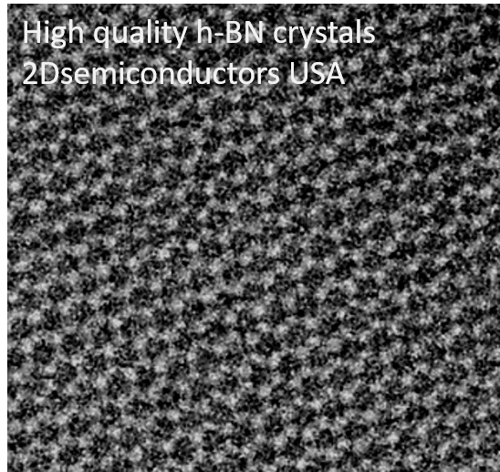
TEM data collected from h-BN monolayers on TEM grids
Raman spectrum of h-BN crystals
Cadhodoluminescence signal from our h-BN crystals
Partial List of Publications Using This Product
C. Ciano et.al. Observation of phonon-polaritons in thin flakes of hexagonal boron nitride on gold; Appl. Phys. Lett. 112, 153101 (2018)
R. Schuster et.al. "Direct observation of the lowest indirect exciton state in the bulk of hexagonal boron nitride" Phys. Rev. B 97, 041201(R) (2018)
J. Ye et.al. "Nonlinear dynamics of trions under strong optical excitation in monolayer MoSe2" Nature Scientific Reports, 8, 2389 (2018)
G. Shepard et.al. "Nanobubble induced formation of quantum emitters in monolayer semiconductors" 2Dmaterials Accepted Manuscript
N. Mishra et.al. "Rapid and catalyst-free van der Waals epitaxy of graphene on hexagonal boron nitride" http://dx.doi.org/10.1016/j.carbon.2015.09.100
A. P. Nayak et. al. "Pressure-Modulated Conductivity, carrier Density, and Mobility of Multilayered Tungsten Disulfide" ACS Nano 10.1021/acsnano.5b03295
Direct observation of the lowest indirect exciton state in the bulk of hexagonal boron nitride; R. Schuster, C. Habenicht, M. Ahmad, M. Knupfer, and B. Büchner Phys. Rev. B 97, 041201(R) 2018
C. Ciano et.al. Observation of phonon-polaritons in thin flakes of hexagonal boron nitride on gold Appl. Phys. Lett. 112, 153101 (2018)
Additional Information
Elements: |
B,N |
Element: |
Boron |
Element: |
Nitrogen |
Formula: |
BN |
Material class: |
Nitride |
Properties: |
Insulator |
Properties: |
Excitonic |
Band gap range: |
UV |
Growth method: |
Atmospheric pressure |
Doping: |
Undoped |
Growth method: |
High pressure |


