Description
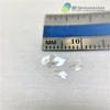
World's largest size h-BN crystals are available! Our h-BN crystals now measure 4-6 mm in size much comparable to other traditional layered crystals. After 3 years of research and engineering, our team has developed state-of-the-art h-BN growth technique (Epitaxial solidification technique© patent pending) to synthesize these large size crystals. In this growth technique, boron and nitrogen elements are first dissolved in our secret metal alloy liquids formula at high temperatures (T>2200C) in RF coils under controlled pressure / environment. Once the precursors are dissolved, the temperature is carefully reduced at designed rates to reject B and N atoms slowly. During the rejection B and N atoms epitaxially bind to seed high quality h-BN crystals to achieve large size h-BN crystals. Once the growth is complete special care is given to purification to ensure 6N purity h-BN crystals with sharp Raman spectra, excellent diffraction pattern, and easy exfoliation characteristics. Since the crystals are large, the exfoliation process is rather simple and monolayers as large as 50-100 um can be achieved using standard exfoliation techniques.
Each order usually contains three or more crystals that measure <5mm in size. Size variations can happen but the crystal sizes will be much larger than anything available commercially or in academia.
If your research needs even larger size h-BN crystal (8-9mm) please reach to us. Our team can arrange dedicated growth to achieve such sizes at additional cost.
Advantages of epitaxial solidifcation technique h-BN growth
- World record size hBN crystals. Reaching 5mm! The first in the commercial market
- Large exfoliated h-BN monolayers. Excellent layered nature and easy exfoliation characteristics enabling getting large monolayer sheets using simple exfoliation
- High purity. Unmatched 6N (99.9999%) secondary ion mass spectroscopy (SIMS) confirmed h-BN crystals.
- Electronic and optical grade
The properties of large size h-BN crystals
| Sample size | Each order usually contains three or more crystals that measure <5mm in size. Size variations can happen but the crystal sizes will be much larger than anything available commercially or in academia. |
| Material properties | 2D dielectric / insulator |
| Production method | Epitaxial solidification technique |
| Characterization methods | SIMS, XRD, EDS, Raman (see product images) |
New publications
"Temperature-Dependent Adhesion in van der Waals Heterostructures"
Advanced Materials
"Electrostatically Tunable Near-Infrared Plasmonic Resonances in Solution-Processed Atomically Thin NbSe2"
Advanced Materials (2021)
https://doi.org/10.1002/adma.202101950
Additional Information
Elements: |
B,N |
Element: |
Boron |
Element: |
Nitrogen |
Formula: |
BN |
Material class: |
Nitride |
Properties: |
Insulator |
Properties: |
Excitonic |
Band gap range: |
UV |
Growth method: |
Epitaxial solidification |
Doping: |
Undoped |


