Description
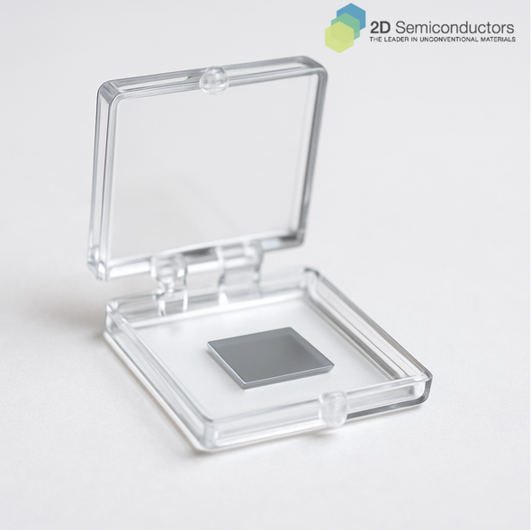
Bulk PdSe2 (palladium diselenide) has been predicted to exhibit 30 meV band gap which increases to 1.43 eV indirect gap (theoretical). It has also been shown to exhibit superconductivity below ~13K under mild hydrostatic pressures, and even semimetallic response in the bulk form. In comparison to other TMDCs, PdSe2 has an uncommon structure: Pd atoms coordinate with four Se atoms, forming a square backbone lattice. It has also been recently shown that PdSe2 monolayer immediately undergo PdSe2 to Pd2Se3 crystal transformation. Owing to vast amount of Pd atoms, PdSe2 has been theoretically and experimentally shown to be catalytically active material thoigh fundamental research still remains at its seminal stages. The product measures 10x10mm in size.
Properties of CVD grown PdSe2
| Material properties | CDW, superconducting, IR-VIS semiconductor, catalytic |
| Crystal structure | Pbca |
| Unit cell parameters | a= 0.579 nm b=0.594 nm, c = 0.859 nm, α=β=γ=90° |
| Growth method | Flux zone growth (contamination halide free) |
| Purity | 99.9999% confirmed |
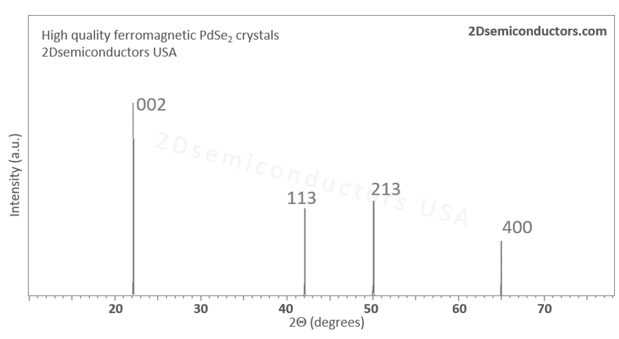
XRD data collected from PdSe2

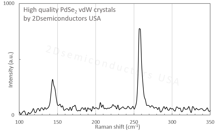
Raman spectrum collected from PdSe2 crystals

Additional Information
Elements: |
Pd,Se |
Element: |
Palladium |
Element: |
Selenium |
Formula: |
PdSe2 |
Material class: |
MX2 |
Material class: |
Dichalcogen |
Properties: |
Semiconductor |
Properties: |
Superconductor |
Properties: |
Semimetal |
Band gap range: |
IR |
Growth method: |
CVD |
Doping: |
Undoped |
Thin-film type: |
Few-layer |
Substrate: |
Sapphire |


