Description
TiS2 exhibits semimetallic behavior, characterized by a slight overlap between its conduction band and valence band. Additionally, it demonstrates diamagnetic properties. The individual layers of TiS2 are assembled through van der Waals interactions and can be easily exfoliated to obtain thin 2D layers.
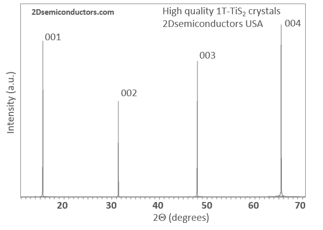
Our TiS2 crystals are stabilized in 1T semi-metallic phase and they are grown using two different techniques through chemical vapor transport (CVT) or flux zone growth (see description of these two methods below). These crystals are treated as gold standards in 2D materials field owing to perfected electronic behavior with guaranteed phase transition and semi-metallic responses. Our TiS2 crystals are notoriously known low impurity resistance (zero temperature resistance), high carrier mobility, extremely clean and sharp XRD peaks, and negligible amount of defects (see published results as well as CVT vs. Flux based methods below ). Our TiS2 crystals are large in size and ready for exfoliation without any preparation.
Properties of vdW TiS2 crystals
| Sample size | Reaching to ~1 cm combined size |
| Material properties | Semimetal |
| Crystal structure | 1T phase a=b=0.338 nm c=0.574 nm |
| Degree of exfoliation | Very easy to exfoliate |
| Production method |
Flux zone growth no contaminations the least grain boundary [Optional] CVT grown crystals halide contamination and more defected. |
| Other characteristics |
|
Growth method matters> Flux zone or CVT growth method? Contamination of halides and point defects in layered crystals are well known cause for their reduced electronic mobility, reduced anisotropic response, poor e-h recombination, low-PL emission, and lower optical absorption. Flux zone technique is a halide free technique used for synthesizing truly semiconductor grade vdW crystals. This method distinguishes itself from chemical vapor transport (CVT) technique in the following regard: CVT is a quick (~2 weeks) growth method but exhibits poor crystalline quality and the defect concentration reaches to 1E11 to 1E12 cm-2 range. In contrast, flux method takes long (~3 months) growth time, but ensures slow crystallization for perfect atomic structuring, and impurity free crystal growth with defect concentration as low as 1E9 - 1E10 cm-2. During check out just state which type of growth process is preferred. Unless otherwise stated, 2Dsemiconductors ships Flux zone crystals as a default choice.
XRD data collected from vdW TiS2 crystals

Publications from this product
H. Yi et.al. The band structure of the quasi-one-dimensional layered semiconductor TiS3(001); Appl. Phys. Lett. 112, 052102 (2018)
Additional Information
Elements: |
Ti,S |
Element: |
Titanium |
Element: |
Sulfur |
Formula: |
TiS2 |
Material class: |
MX2 |
Material class: |
Dichalcogen |
Properties: |
Semiconductor |
Properties: |
Excitonic |
Properties: |
Metal |
Band gap range: |
VIS |
Growth method: |
Flux |
Growth method: |
CVT |
Doping: |
Undoped |


