Description
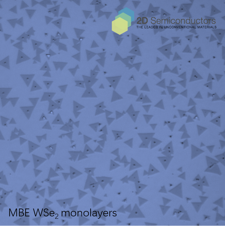
World's first molecular beam epitaxy (MBE) grown WSe2 monolayers. MBE is an epitaxial method for single-crystal quality film deposition which offers high crystallinity and reduced defect density compared to chemical vapor deposition (CVD) or metal-organic chemical vapor deposition (MOCVD) techniques (see HRTEM images below). MBE growth of WSe2 monolayers take place in a MBE chamber at a base pressure of 8E-9 Torr and deposition rate is extremely slow (5-100 atoms per second) to reach structural perfection. Typical MBE growth produces monolayer thick WSe2 isolated triangles on double-side polished c-cut sapphire. Currently, MBE WSe2 is only offered on sapphire substrates but in the near future our MBE substrates will also include mica, graphite, and gold.
Comparison between MBE, CVD, and MOCVD

TEM comparison between MBE, CVD, and MOCVD

Optical images collected from MBE WSe2

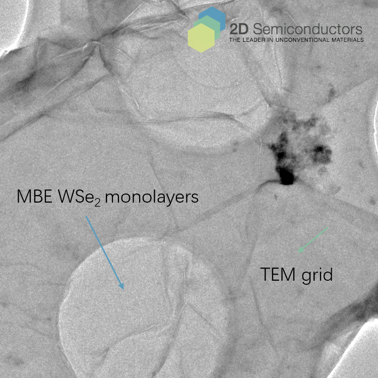
MBE WSe2 suspended on TEM grid

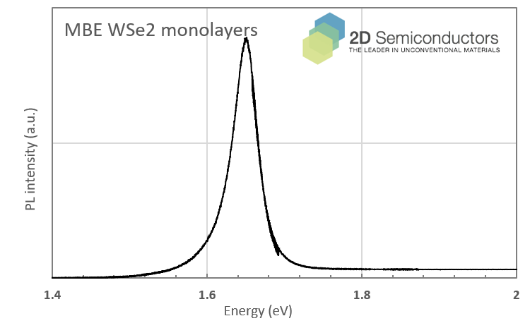
PL spectrum collected from MBE WSe2

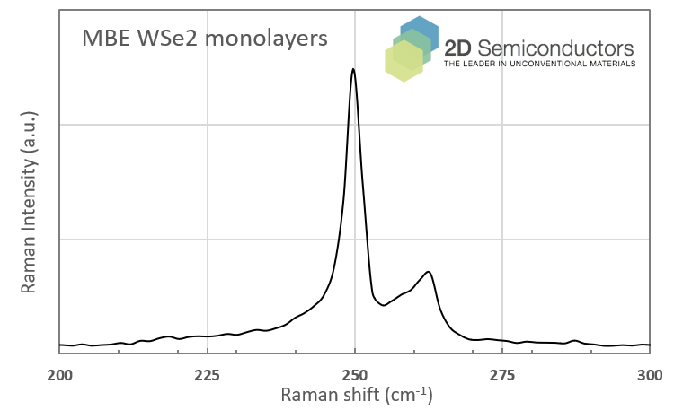
Raman spectrum collected from MBE WSe2

Additional Information
Elements: |
W,Se |
Element: |
Tungsten |
Element: |
Selenium |
Formula: |
WSe2 |
Substrate: |
Sapphire |
Thin-film type: |
Triangles |
Material class: |
Dichalcogen |
Properties: |
Semiconductor |
Growth method: |
MBE |
Thin-film type: |
Monolayer |
Band gap range: |
VIS |
Properties: |
Excitonic |
Material class: |
MX2 |


