Description
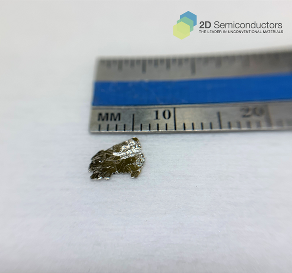
We provide the world's largest size commercially available In2Se3 crystals at the highest quality In2Se3 and affordable prices. Our crystals exceed competing crystals both in size and quality. All the crystals come exfoliation ready.
In2Se3 single crystals were grown using Bridgman or chemical vapor transport (CVT) techniques. These crystals are largest in the commercial market with high attention given to having best electronic and optical quality. Unlike other In2Se3, the phase of this product is controlled carefully by after meticulous synthesis refinement steps and the flakes are highly crystalline. Flakes are perfectly layered, in-plane sheets are perfectly aligned in the (002) direction as determined by XRD and 4-angle XRD (rocking curves). In the bulk, the crystals display 1.41 eV band gap and show strong Raman peaks.
Properties of In2Se3 layered crystals
| Material properties | Semiconducting |
| Crystal structure | Hexagonal |
| Unit cell parameters | a=b=0.34 nm, c=18.84 nm; α=β=90°, γ=120° |
| Growth method | Float zone technique or chemical vapor transport |
| Purity | 99.9999% guaranteed |
| Characterization | XRD, XPS, AES, SIM, and HRTEM |
XRD spectrum from In2Se3 layered crystals

Recent work citing our crystal
Stacking selected polarization switching and phase transition in vdW ferroelectric α-In2Se3 junction devices
Nature Communications, 15, 10481 (2024)
An optoelectronic synapse based on α-In2Se3 with controllable temporal dynamics for multimode and multiscale reservoir computing
Nature Electronics, 5, 761–773 (2022)
Ultrathin two-dimensional van der Waals asymmetric ferroelectric semiconductor junctions featured
Journal of Applied Physics 132, 054101 (2022)
Understanding Microscopic Operating Mechanisms of a van der Waals Planar Ferroelectric Memristor
Advanced Functional Materials 2021
https://doi.org/10.1002/adfm.202009999
An optoelectronic synapse based on In2Se3 with controllable temporal dynamics for multimode and multiscale reservoir computing
Nature Electronics (2022)
Additional Information
Elements: |
In,Se |
Element: |
Indium |
Element: |
Selenium |
Formula: |
In2Se3 |
Material class: |
M2X3 |
Properties: |
Semiconductor |
Band gap range: |
IR |
Band gap range: |
VIS |
Growth method: |
Float zone |
Doping: |
Undoped |


