Description
World's largest size highest quality MoO3 crystals
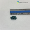
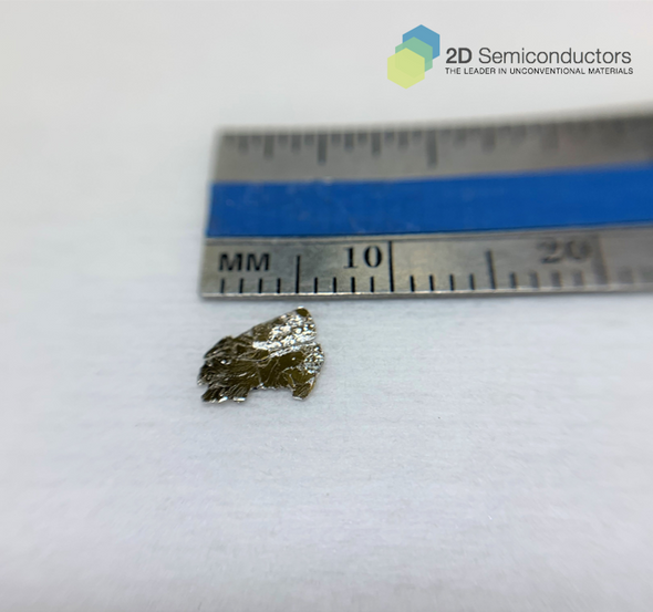
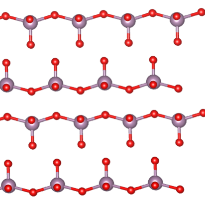
a-MoO3 is a layered vdW semiconductor with a crystal structure that belongs to the space group Pbnm 62 (see unit cell parameters below). It is layered and as easy to exfoliate as MoS2 or graphite. In its layered form, Each layer has three atomic thick arrangement consisting of MoO6 octahedra layers as shown in the diagram in product images. The material is environmentally stable in air, water, and different gases. Layers can easily exfoliated onto desired substrates with minimal efforts as shown in the product images. Bridgman grown crystals are larger in size and higher in quality.
General characteristics of a-MoO3 crystals
| Sample size | Each order contains large sized crystals (see images) |
| Material properties | 2D oxide, quantum emitter, 2D insulator |
| Crystal structure | a-phase |
| Degree of exfoliation | Easy to exfoliate |
| Production method | Bridgman (recommended) or CVT growth Bridgman crystals are higher crystal quality and purity |
| Other characteristics |
|
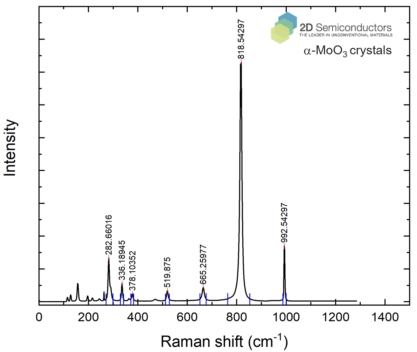
Raman spectrum collected from high crystalline MoO3 crystals
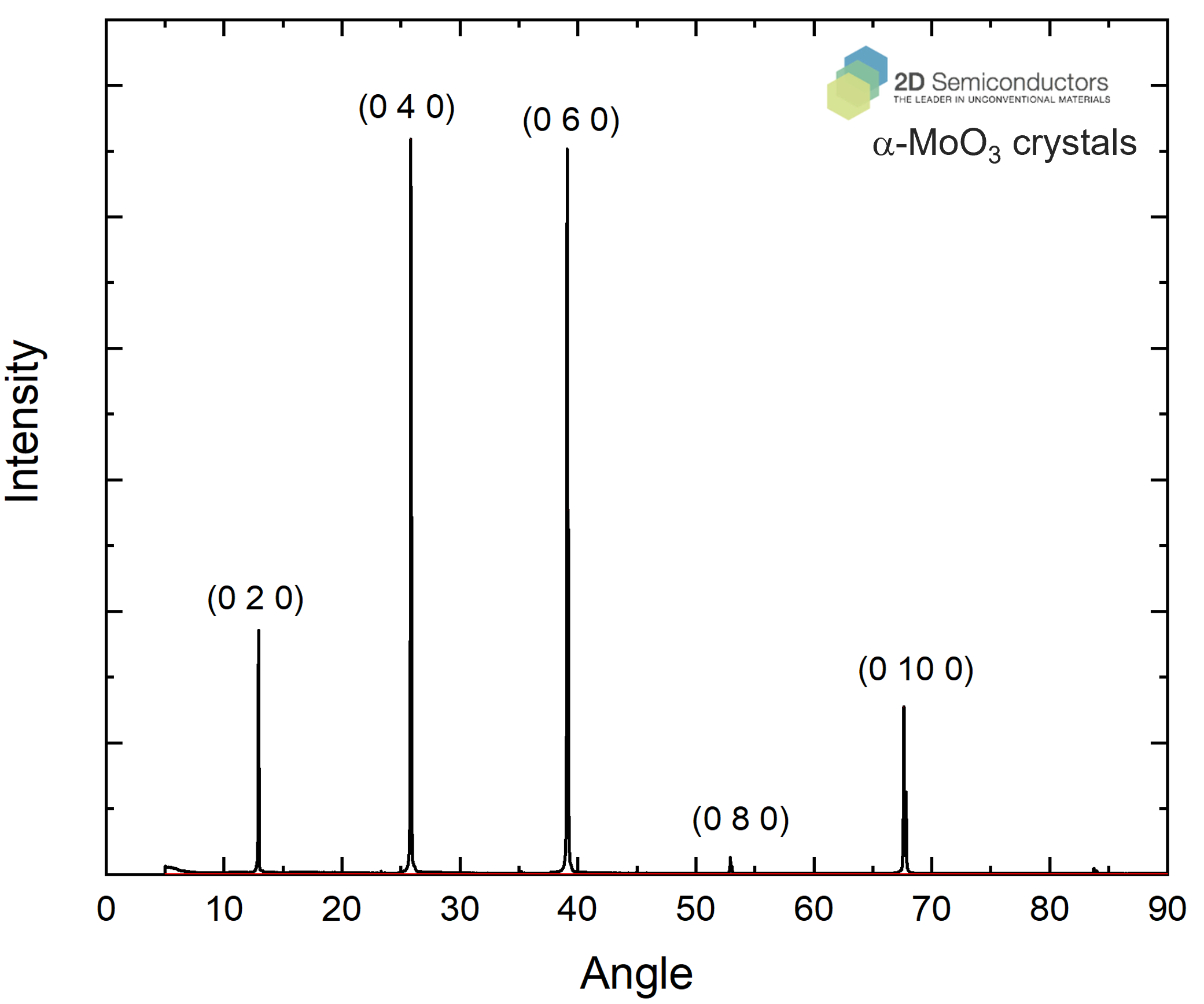
XRD data collected from MoO3 crystals
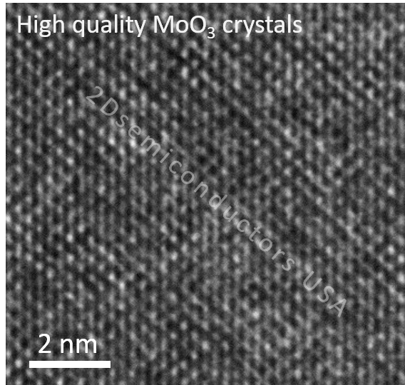
Transmission electron microscopy characterization on MoO3 crystals
Atomic depiction of MoO3 layers
References
Low-Loss Anisotropic Image Polaritons in van der Waals Crystal α-MoO3
Advanced Optical Materials
https://doi.org/10.1002/adom.202201492
Nanoscale‐Confined Terahertz Polaritons in a van der Waals Crystal,
Advanced Materials doi.org/10.1002/adma.202005777 (2020)
Kitchaev et.al. Phys. Rev. B 93, 045132 (2016)
Additional Information
Elements: |
Mo,O |
Element: |
Molybdenum |
Element: |
Oxygen |
Formula: |
MoO3 |
Material class: |
MX3 |
Material class: |
Oxide |
Material class: |
Quasi-1D |
Properties: |
Semiconductor |
Properties: |
Excitonic |
Band gap range: |
VIS |
Band gap range: |
UV |
Growth method: |
Bridgman |
Growth method: |
CVT |
Doping: |
Undoped |


