Description
We provide the world's largest size (guaranteed or money back) SnS2 crystals at the highest quality SnS2 and affordable prices. Our crystals exceed competing crystals both in size and quality.
Our newly patented modified Bridgman-Levy technique also offers "Levy/Bridgman" SnS2 crystals with superior performance compared to CVT grown (commonly used by other commercial suppliers) SnS2. These crystals offer excellent surface finish, ultimate layer stacking, 7N or higher purity, and lowest defect density (1E9cm-2 or better)
Advantages of our SnS2 crystals
- World's largest size (guaranteed) SnS2 crystals
- World's only Levy/Bridgman modified SnS2 crystals for superior electronic and optical performance
- Defect levels at record 1E-9cm-2 ranges
- Purity level (RBS and SIMS confirmed) at 7N
- 20 years of continous optimization for superior performance.
C2DB database [Link]
Characteristics of SnS2 crystals
| Crystal size | 10 mm or larger (Record size) |
| Material properties | Indirect gap semiconductor |
| Crystal structure |
Hexagonal |
| Unit cell parameters | a=b=0.368 nm, c=0.582 nm; α=β=90° γ=120° |
| Growth method | [Default] Flux zone (no halide contamination) defect free [Optional CVT]: Contains Br2, Cl2, TeCl4, and other halides |
| Purity | 99.9999% confirmed |
Growth method matters> Flux zone or CVT growth method? Contamination of halides and point defects in layered crystals are well known cause for their reduced electronic mobility, reduced anisotropic response, poor e-h recombination, low-PL emission, and lower optical absorption. Flux zone technique is a halide free technique used for synthesizing truly semiconductor grade vdW crystals. This method distinguishes itself from chemical vapor transport (CVT) technique in the following regard: CVT is a quick (~2 weeks) growth method but exhibits poor crystalline quality and the defect concentration reaches to 1E11 to 1E12 cm-2 range. In contrast, flux method takes long (~3 months) growth time, but ensures slow crystallization for perfect atomic structuring, and impurity free crystal growth with defect concentration as low as 1E9 - 1E10 cm-2. During check out just state which type of growth process is preferred. Unless otherwise stated, 2Dsemiconductors ships Flux zone crystals as a default choice.
Raman spectrum collected from SnS2 vdW crystals

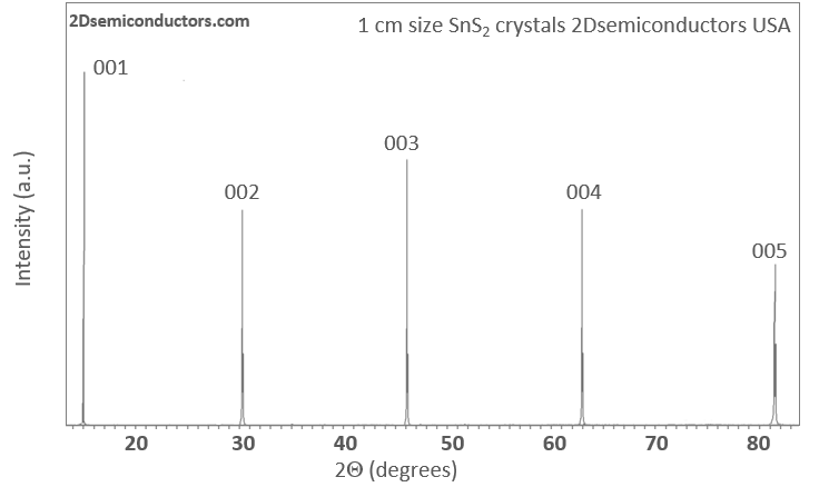
XRD data collected from SnS2 vdW crystals

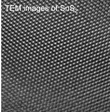
HRTEM Data taken from SnS2 vdW Crystals

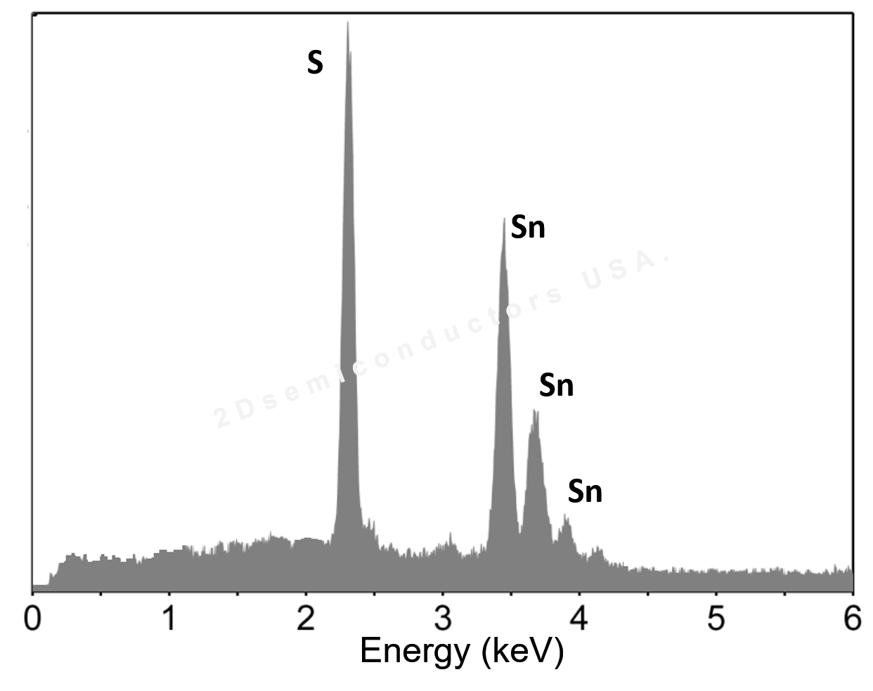
EDS data collected from SnS2 crystals

Additional Information
Elements: |
Sn,S |
Element: |
Tin |
Element: |
Sulfur |
Formula: |
SnS2 |
Material class: |
MX2 |
Properties: |
Semiconductor |
Band gap range: |
VIS |
Growth method: |
Flux |
Growth method: |
CVT |
Doping: |
Undoped |


