Description
We provide the world's largest size commercially available SnSe2 crystals at the highest quality SnSe2 and affordable prices. Our crystals exceed competing crystals both in size and quality. SnSe2 crystals come with three options Bridgman grown (highest grade but smaller in size), Flux or CVT grown (more than 1cm in size but slightly lower grade)
Description
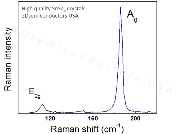
World-record-size single crystal SnSe₂ (Tin diselenide) crystals have been developed at our facilities using state-of-the-art techniques. All the crystals are ready for exfoliation, as shown in the images. These crystals are larger than 1 cm in size, providing ample material to work with. In bulk form, SnSe2 is a 1.0 eV direct band gap semiconductor, and in monolayer form, it becomes a 1.4 eV direct semiconductor. Our crystals exhibit high crystallinity, with very sharp Raman peak signals at 109 and 182 cm-1 and a full width at half maximum (FWHM) of less than 4 cm-1. They are produced at our facilities using three different techniques: Bridgman growth (highest grade), Flux, or CVT growth (lower grade). Each growth process takes close to three months to yield perfected crystals that do not contain any halides. Each crystal is large in size, ensuring longevity for research purposes, and is highly crystalline, oriented in the 0001 direction, and easy to exfoliate. Our R&D staff collects characterization datasets for each sample piece to ensure structural, optical, and electronic consistency.
Characteristics of SnSe2 crystals
| Crystal size | ~1 cm |
| Unit cell perameters | a=b=0.380, c=0.618 nm; α=β=90°, γ=120° |
| Material properties | Semiconducting |
| Crystal structure | Hexagonal phase |
| Growth method | [Default] Flux zone (no halide contamination) defect free [Optional CVT]: Contains Br2, Cl2, TeCl4, and other halides |
| Purity | 99.9999% confirmed |
| Characterization | XRD,XPS,AES,SIM, and HRTEM |
Growth method matters> Flux zone or CVT growth method? Contamination of halides and point defects in layered crystals are well known cause for their reduced electronic mobility, reduced anisotropic response, poor e-h recombination, low-PL emission, and lower optical absorption. Flux zone technique is a halide free technique used for synthesizing truly semiconductor grade vdW crystals. This method distinguishes itself from chemical vapor transport (CVT) technique in the following regard: CVT is a quick (~2 weeks) growth method but exhibits poor crystalline quality and the defect concentration reaches to 1E11 to 1E12 cm-2 range. In contrast, flux method takes long (~3 months) growth time, but ensures slow crystallization for perfect atomic structuring, and impurity free crystal growth with defect concentration as low as 1E9 - 1E10 cm-2. During check out just state which type of growth process is preferred. Unless otherwise stated, 2Dsemiconductors ships Flux zone crystals as a default choice.
Raman spectrum collected from SnSe2 vdW crystals

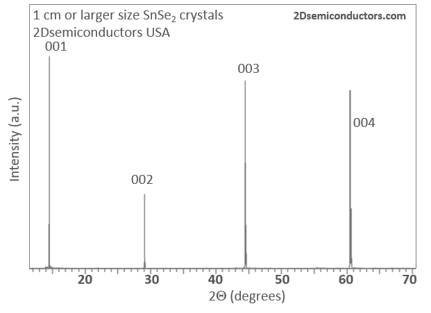
XRD data collected from SnSe2 vdW crystals

HRTEM Data taken from SnSe2 vdW Crystals

Recent work citing our crystals
Negative Differential Photoconductance as a Signature of Nonradiative Energy Transfer in van der Waals Heterojunction
ACS Nano 2021, 15, 10, 16432–16441
Additional Information
Elements: |
Sn,Se |
Element: |
Tin |
Element: |
Selenium |
Formula: |
SnSe2 |
Material class: |
MX2 |
Material class: |
Dichalcogen |
Properties: |
Semiconductor |
Band gap range: |
VIS |
Growth method: |
Flux |
Growth method: |
CVT |
Doping: |
Undoped |
Growth method: |
Bridgman |


