Description
2H-phase TaSe2 is a 2D superconductor with critical temperature (Tc) of 0.32K, and exhibit incommensurate charge density waves (CDW) around 90K. Its metallic vs. semimetallic behavior is also under debate. Our crystals are grown by either flux zone method to achieve defect free crystals or CVT method which is known to introduce halide contaminants in the crystal. By default, we ship flux zone 2H-TaSe2 crystals with guaranteed superconducting and CDW behavior (the only commercially vdW TaSe2 crystals with guaranteed CDW and SC behavior). Our crystals are environmentally stable which means that they can be handled safely under ambient conditions without any need for chemical fume hood or inert glove box.
Flux zone vs. CVT growth method: Contamination and defects in TaSe2 crystals are well known to influence CDW behavior. (temperature onset, ability to observe, sheet resistance). Flux zone technique is a halide free and slow growth technique used for synthesizing truly electronic grade vdW crystals. This method distinguishes itself from chemical vapor transport (CVT) technique provides quick (~2 weeks) growth but poor crystalline quality while flux method takes ~3 months, ensures slow crystallization for perfect atomic structuring, and impurity free crystal growth. During check out just state which type of growth process is preferred. Unless otherwise stated, 2Dsemiconductors ships Flux zone crystals as default choice.
Properties of 2H phase TaSe2 crystals - 2Dsemiconductors USA
| TaS₂ (2H phase) | CDW (~90K), metal, semimetal, low T꜀ superconductor (T<1K) |
| Crystal structure | Hexagonal phase |
| Unit cell perameters | a=b=0.338 nm, c=1.262 nm; α=β=90°, γ=120° |
| Growth method | Flux zone (guaranteed CDW response) [On request: chemical vapor transport (CVT) may contain Br2, Cl2, TeCl4, and other halides] |
| Purity | 99.9999% confirmed |
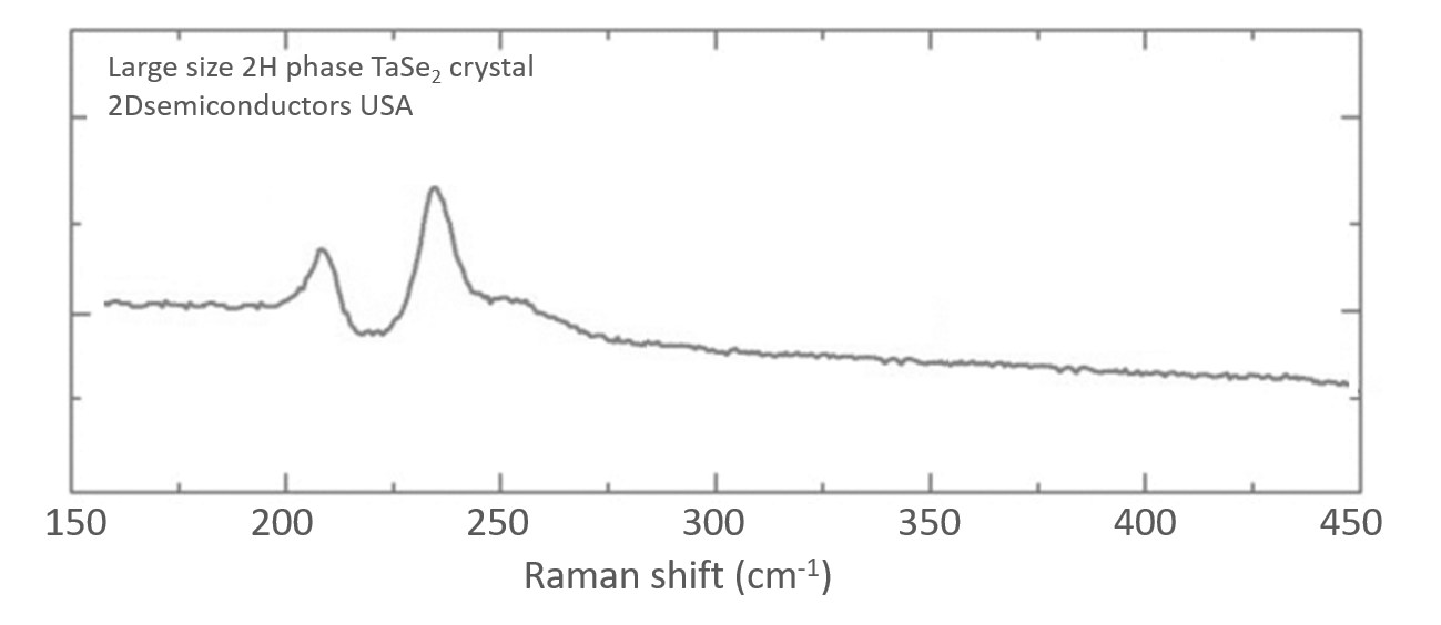
Raman data from 2H phase TaSe2 crystals - 2Dsemiconductors USA

Plasmons in the van der Waals charge-density-wave material 2H-TaSe2
Nature Communications volume 12, Article number: 386 (2021)
Negative Differential Photoconductance as a Signature of Nonradiative Energy Transfer in van der Waals Heterojunction
ACS Nano 2021, 15, 10, 16432–16441
H. Ryu et.al. "Persistent Charge-Density-Wave Order in Single-Layer TaSe2" Nano Letters, 18, 689 (2018)
Additional Information
Elements: |
Ta,Se |
Element: |
Tantalum |
Element: |
Selenium |
Formula: |
TaSe2 |
Material class: |
MX2 |
Material class: |
Dichalcogen |
Properties: |
Semiconductor |
Properties: |
Superconductor |
Properties: |
Semimetal |
Properties: |
CDW |
Band gap range: |
VIS |
Growth method: |
Flux |
Growth method: |
CVT |
Doping: |
Undoped |


