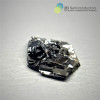
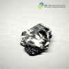
Description
At 2D Semiconductors, we offer the largest, highest-quality WSe2 van der Waals (vdW) crystals available, recognized as gold standards in the field. Our WSe₂ crystals are grown using two advanced methods, Chemical Vapor Transport (CVT) and Flux Zone Growth (Flux), each tailored to produce specific properties and exceptional performance characteristics. All our WSe2 crystals come with guaranteed excitonic, photoluminescence (PL), and electronic properties.
Flux Grown WSe2 Crystals:
Our Flux-grown WSe2 crystals boast outstanding electronic and valleytronic performance, with perfect crystallization and defect-free structures. These crystals feature extremely narrow PL bandwidths, clean PL spectra free from bound exciton shoulders, and exceptional carrier mobility. The most recent crystals exceed 1 cm in size, offering unparalleled quality for high-performance applications.
CVT Grown WSe2 Crystals:
While CVT-grown WSe2 crystals maintain impressive size, often exceeding 1 cm, they offer electronic and optical properties more comparable to commercially available materials. These crystals may have some defects and slightly lower performance metrics in comparison to Flux-grown samples, making them a cost-effective option for certain applications.
p and n-type crystals: p- and n-type crystals inherently smaller in size due to difficulty in their synthesis and low crystal yield rates. Typical size is around 5 to 10 mm.
For premium ultra flat large size (~2cm) WSe2 crystals follow the link here [Link]
![]() Materials Project WSe2
Materials Project WSe2
![]() C2DB material properties WSe2
C2DB material properties WSe2
| Crystal Size | Larger than 1 cm in size - Guaranteed size |
| Dopants | Undoped (intrinsic semiconductor), Please also see our n- and p-type WSe2 crystals doped with Au, Re, Nb, or other transition metal atoms. |
| Material properties | 1.62 eV emission (300k), direct gap semiconductor |
| Crystal structure | Hexagonal phase |
| Unit cell perameters | a = b = 0.331 nm, c - 1.298 nm, α=β=90°, y=120° |
| Growth methods | Flux zone (no halide contamination) defect free. CVT, contains Br₂, Cl₂, TeCl₄ and other halides |
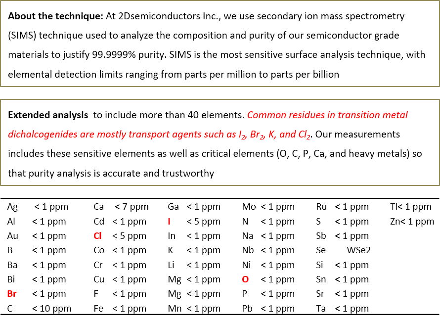
| Purity | 99.9999% confirmed |
Growth method matters> Flux zone or CVT growth method? Contamination of halides and point defects in layered crystals are well known cause for their reduced electronic mobility, reduced anisotropic response, poor e-h recombination, low-PL emission, and lower optical absorption. Flux zone technique is a halide free technique used for synthesizing truly semiconductor grade vdW crystals. This method distinguishes itself from chemical vapor transport (CVT) technique in the following regard: CVT is a quick (~2 weeks) growth method but exhibits poor crystalline quality and the defect concentration reaches to 1E11 to 1E12 cm-2 range. In contrast, flux method takes long (~3 months) growth time, but ensures slow crystallization for perfect atomic structuring, and impurity free crystal growth with defect concentration as low as 1E9 - 1E10 cm-2. During check out just state which type of growth process is preferred. Unless otherwise stated, 2Dsemiconductors ships Flux zone crystals as a default choice. Combined crystal size reaches to ~cm.
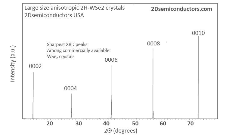
XRD data collected from WSe2 crystals
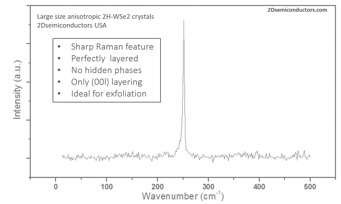
Raman spectrum collected from WSe2 monolayers
Photoluminecence spectrum collected from monolayer WSe2 exfoliated from WSe2 crystals

SIMS purity datasets collected from WSe2 crystals
HRTEM images collected from WSe2 crystals

Partial List of Publications from This Product
Summary: Publications from MIT, Washington, MIT, Berkeley, Stanford, and Princeton teams at top journals like Nature Physics, Nature Nanotechnology, Nature Communications, Nano Letters, and Advanced Materials
Enabling valley selective exciton scattering in monolayer WSe2 through upconversion
Nature Communications volume 8, Article number: 14927 (2017), doi:10.1038/ncomms14927
Spin/valley pumping of resident electrons in WSe2 and WS2 monolayers
Nature Communications volume 12, Article number: 5455 (2021)
Enabling valley selective exciton scattering in monolayer WSe2 through upconversion, Nature Communications, 8,14927 (2017)
doi:10.1038/ncomms14927
Control of Exciton Valley Coherence in Transition Metal Dichalcogenide Monolayers, Phys. Rev. Lett. 117, 187401 (2016)
Washington University - G. Aivazian et.al. "Magnetic control of valley pseudospin in monolayer WSe2" Nature Physics 11, 148–152 (2015)
Berkeley - M. Zhao et.al. "Large-scale chemical assembly of atomically thin transistors" Nature Nanotechnology 11, 954–959 (2016)
Tony Heinz – Stanford / Columbia University
Measurement of the optical dielectric function of monolayer transition-metal dichalcogenides: MoS2, MoSe2, WS2, and WSe2, Yilei Li, Alexey Chernikov, Xian Zhang, Albert Rigosi, Heather M. Hill, Arend M. van der Zande, Daniel A. Chenet, En-Min Shih, James Hone, and Tony F. Heinz; Phys. Rev. B 90, 205422 (2014)
Andras Kis EPFL team "Valley Polarization by Spin Injection in a Light-Emitting van der Waals Heterojunction" Nano Letters 2016, 16, 5792−5797
Z. Li et. al. Layer Control of WSe2 via Selective Surface Layer Oxidation; ACS Nano, 2016, 10 (7), pp 6836–6842
Giant Enhancement of the Optical Second-Harmonic Emission of WSe2, Monolayers by Laser Excitation at Exciton Resonances; G. Wang, X. Marie, I. Gerber, T. Amand, D. Lagarde, L. Bouet, M. Vidal, A. Balocchi, and B. Urbaszek; Phys. Rev. Lett. 114, 097403 (2016)
M. Yankowitz et. al. "Intrinsic Disorder in Graphene on Transition Metal Dichalcogenide Heterostructures" Nano Letters, 2015, 15 (3), pp 1925–1929
Tongay et. al. "Defects activated photoluminescence in two-dimensional semiconductors: interplay between bound, charged, and free excitons" Scientific Reports 3, Article number: 2657 (2013)
T. Yan et. al. "Valley depolarization in monolayer WSe2" Scientific Reports 5, Article number: 15625 (2015)
G. Wang et.al. "Valley dynamics probed through charged and neutral exciton emission in monolayer WSe2" Phys. Rev. B 90, 075413 (2015)
X Li et al. "Determining layer number of twodimensional flakes of transition-metal dichalcogenides by the Raman intensity from substrates" Nanotechnology 27 (2016) 145704
J. Wu- UC, Berkeley Anomalous Raman spectra and thickness-dependent electronic properties of WSe2 H. Sahin, S. Tongay, S. Horzum, W. Fan, J. Zhou, J. Li, J. Wu, and F. M. Peeters; Phys. Rev. B 87, 165409 (2013)
Duke University J. Huang et. al. "Probing the origin of excitonic states in monolayer WSe2" Scientific Reports 6, Article number: 22414 (2016)
Manish Chhowalla, "Two-dimensional semiconductors for transistors" Nature Reviews Materials 1, Article number: 16052 (2016) doi:10.1038/natrevmats.2016.52
Y. Li "Ultrafast Interlayer Electron Transfer in Incommensurate Transition Metal Dichalcogenide Homobilayers" Nano Lett., 2017, 17 (11), pp 6661–6666
G. Shepard et.al. "Nanobubble induced formation of quantum emitters in monolayer semiconductors" 2Dmaterials Accepted Manuscript
L. Zhang. et.al. "Photonic-crystal exciton-polaritons in monolayer semiconductors" Nature Communications volume 9, Article number: 713 (2018)
Enhanced Hole Injection Into Single Layer WSe2 DOI: 10.1109/JEDS.2018.2802929 (2018)
Additional Information
Elements: |
W,Se |
Element: |
Tungsten |
Element: |
Selenium |
Formula: |
WSe2 |
Material class: |
MX2 |
Material class: |
Dichalcogen |
Properties: |
Semiconductor |
Properties: |
Excitonic |
Band gap range: |
VIS |
Growth method: |
CVT |
Growth method: |
Flux |
Doping: |
Undoped |
Doping: |
p-Type |
Doping: |
n-Type |


