Description
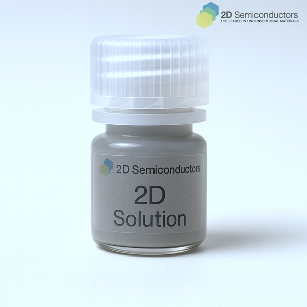
This product contains WSe2 flakes solution in ethanol or any media of your interest. The WSe2 solution has been developed by ultrasonic treatment of bulk WSe2 high quality crystals synthesized through vapor transport (CVT) technique. Since the starting material (CVT grown WSe2 crystals) is highly crystalline, ultrasonic treatment to delaminate WSe2 layers yields highly crystalline WSe2 mono-, few-, and some thick layers suspended in ethanol solution. The crystallinity of WSe2 nanomaterials has been confirmed through electron energy dispersive spectroscopy (EDAX), Raman spectroscopy (FWHM<5 cm-1), and scanning electron microscopy (SEM) measurements. Depending on the thickness of the layers, flakes deposited on different substrates produce light emission (photoluminescence). Lateral sizes of WSe2 flakes deposited onto different substrates range from ~10nm - ~10 mm while thickness range from 1L to 10s of layers.
Note on volume, concentration, and solvent type: To reduce shipping costs, we ship supersaturated 2D solutions (~80-120 mg/L depending on the type of 2D layers). However, supersaturated solutions can be diluted to produce ~250-500mL of solution to deposit 2D layers onto desired substrates through simple and cost-effective spin-casting process. In our product, ethanol is used (and recommended) as the dispersant solvent owing to its environmental stability, thermal stability, dispersant properties, and non-contaminating nature. However, if your research needs other solvents, please contact us at support_at_2dsemiconductors.com
Sample Properties
| Sample amount | Designer concentration [Standard:1mg/mL] 8mL or larger quantities |
| Solution type | Ethanol (highly recommended) [see notes above] |
| Thickness / size range | 1 to 10s of layers in thickness / 10nm-10mm in lateral size |
| Fundamental properties | 1.62 eV Direct Bandgap Semiconductor |
| Crystal structure | Hexagonal Phase |
| Unit cell parameters | a=b=0.327 nm, c=1.295 nm; α=β=90°, γ=120° |
| Production method | Ultrasonic treatment assisted delamination of WSe2 crystals |
| Characterization methods | Raman, EDS, AFM, SEM (contact us for more information) |
Specifications
- Identification. WSe2 solutions created by delamination of WSe2 crystals (grown by CVT method) through ultrasonication technique
- Physical dimensions. 1 to 10 layers in thickness (thicker pieces might be observed depending on usage) and 10nm to 10 microns in lateral dimensions.
- Smoothness. Atomically smooth surface with roughness < 0.35 nm.
- Purity. 99.999% purity as determined by nano-SIMS measurements
- Stability. High environmental and dispersant stability.
- Crystallinity. Highly crystalline nanomaterials. No amorphous sheets, contaminants, or hidden secondary phases.
- Dispersant solution. Ethanol is highly recommended though other solvents can be prepared on demand.
- Support. 2Dsemiconductors USA is an American owned, regulated, and operated company. Our customers are well-protected by international as well as strict American customer laws and regulations. We give full technical support and guarantee your satisfaction with our well-established customer
Supporting datasets
Scanning electron microscope images taken from WSe2 solution deposited onto SiO2/Si substrates [Left] Dense limit and [Right] Dilute limit


EDS elemental composition data collected from WSe2 solutions

Raman spectroscopy data collected from variety of 2D solutions

Frequently asked questions
Q1: Are these solutions good for catalytic measurements?
A: Yes, our 2D solutions are commonly used by catalysis community
Q2: What is the volume of the solution?
A: Each order can either contain 2mL of supersaturated monolayer solution (~200mg/L) or dense 20mL solutions (~20mg/L). We recommend using 2mL solutions as this will cut down the shipping charges and shipping times.
Q3: Are these 2D solutions consist of 100% monolayers?
A: This will depend on your requirements. We can design monolayer, few-layer, multi-layer, and even bulk layered solutions. Please identify what kind of solution (material type) you prefer to use during check out.
Q4: How about the solution types?
A: This will also depend on your application. We have capability to accommodate IPA, H2O, DMF, NMP, and many others. Just let us know what you have in mind.
Additional Information
Elements: |
W,Se |
Element: |
Tungsten |
Element: |
Selenium |
Formula: |
WSe2 |
Material class: |
MX2 |
Material class: |
Dichalcogen |
Properties: |
Semiconductor |
Properties: |
Excitonic |
Band gap range: |
VIS |
Growth method: |
Solution Phase |
Doping: |
Undoped |
Solution Type: |
Isopropanol |
Solution Type: |
Ethanol |
Solution Type: |
DI Water |
Solution Type: |
NMP |
Solution Type: |
Custom |


