Description
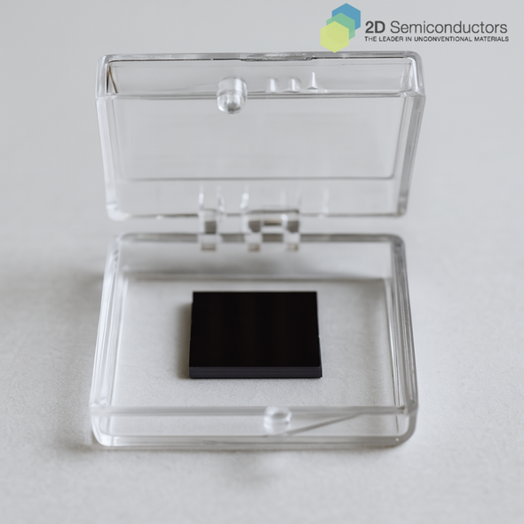
Monolayer graphene transferred on SiO2/Si substrates. Full area graphene monolayers were synthesized first using our established CVD growth method (see below) on copper foils and transferred from copper onto SiO2/Si using copper etchant and polymer assisted stamping technique. The process is optimized to reduce transfer related defects to reach optical and electronic quality. Sample size measures 1cm in size but larger sizes or designer sizes are available upon request. Due to the transfer process, the transferred monolayers may contain natural wrinkles and missing patches in some regions. The entire process is carried under Argon backfilled glovebox to ensure high-quality and residue free process. The samples are always sealed under Argon and pumped down to 1E-6 Torr to deliver quality samples for your research.
Graphene growth method. CVD Graphene sheets have been deposited onto 50 micron thick Cu foils using modified chemical vapor technique. In our method, we have paid close attention to engineering defect density and single domain sizes. Most CVD graphene chambers produce small (100nm - 1um) graphene sheets. Our process parameters have been optimized to reduce the point defect (vacancy) concentration, improve crystallinity, increase single domain size, and reduce 1D grain boundary defect density. Our CVD graphene products undergo weekly routine quality control tests to ensure the growth system is accurate and parameters are up to date.
If your research needs designer 2D superlattices please see our transferred monolayer product line.
Additional Information
Elements: |
C |
Element: |
Carbon |
Formula: |
C |
Material class: |
Carbon |
Properties: |
Metal |
Properties: |
Dirac metal |
Growth method: |
CVD |
Doping: |
Undoped |
Thin-film type: |
Monolayer |
Substrate: |
SiO2/Si |


