Description
Premium Ultra-Flat Large-Area WSe2 Crystals for large area exfoliation
After over five years of dedicated R&D, we are proud to offer our Ultra-Flat Large-Area WSe2 Crystals—precision-engineered specifically for monolayer exfoliation techniques such as Au-assisted transfer. These synthetic crystals represent the highest quality and largest format WSe2 available globally.
Produced using our flagship flux growth method, each crystal measures approximately 2 cm and features unmatched surface flatness, making them ideal for advanced electronic, optical, and quantum applications.
Please note: availability is extremely limited due to the specialized synthesis process.
![]() Materials Project WSe2
Materials Project WSe2
![]() C2DB material properties WSe2
C2DB material properties WSe2
| Crystal Size | Ultra-flat crystals ~2cm size |
| Dopants | Undoped (intrinsic semiconductor) |
| Material properties | 1.62 eV emission (300k), direct gap semiconductor |
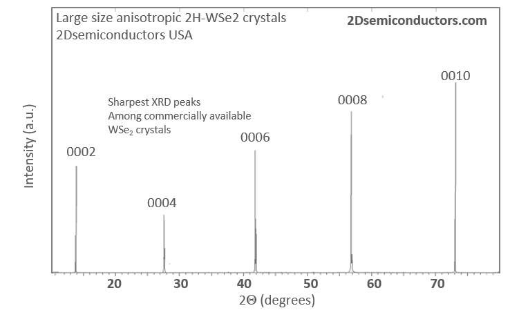
| Crystal structure | Hexagonal phase |
| Unit cell perameters | a = b = 0.331 nm, c - 1.298 nm, α=β=90°, y=120° |
| Growth methods | Flux zone (no halide contamination) defect free. |
| Purity | 99.9999% confirmed |
XRD data collected from WSe2 crystals

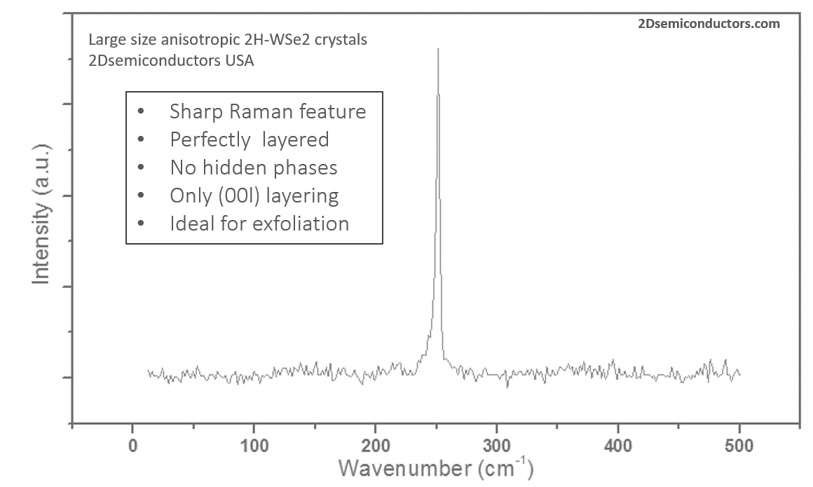
Raman spectrum collected from WSe2 monolayers

Photoluminecence spectrum collected from monolayer WSe2 exfoliated from WSe2 crystals

Additional Information
Elements: |
W,Se |
Element: |
Tungsten |
Element: |
Selenium |
Formula: |
WSe2 |
Material class: |
MX2 |
Material class: |
Dichalcogen |
Material class: |
Alloy |
Properties: |
Semiconductor |
Properties: |
Excitonic |
Band gap range: |
VIS |
Growth method: |
Flux |
Doping: |
Undoped |


