


Description
Limited Edition Ultra-Flat Large-Area MoS2 Crystals
After over five years of dedicated R&D, we are proud to offer our Ultra-Flat Large-Area MoS₂ Crystals—precision-engineered specifically for monolayer exfoliation techniques such as Au-assisted transfer. These synthetic crystals represent the highest quality (TEM, Raman, PL, XRD), purity (SIMS analysis) and largest single crystal size MoS2 available globally.
Produced using our proprietary flagship flux growth method, each crystal measures approximately 3 cm and features unmatched surface flatness, making them ideal for advanced electronic, optical, and quantum applications.
Please note: availability is extremely limited due to the specialized synthesis process.
If your research needs 3R-MoS2 crystals, they can be found in the [link]
The properties of Ultra-Flat Large-Area MoS2 Crystals
| Sample size | Approximately 3cm in size |
| Material properties | Bulk 1.2 eV indirect and Excitonic semiconductor (~1.85 eV) |
| Crystal structure | 2H semiconducting phase |
| Degree of exfoliation | Easy to exfoliate, ideal for large area exfoliation |
| Production method | Flux zone |
| Other characteristics |
|
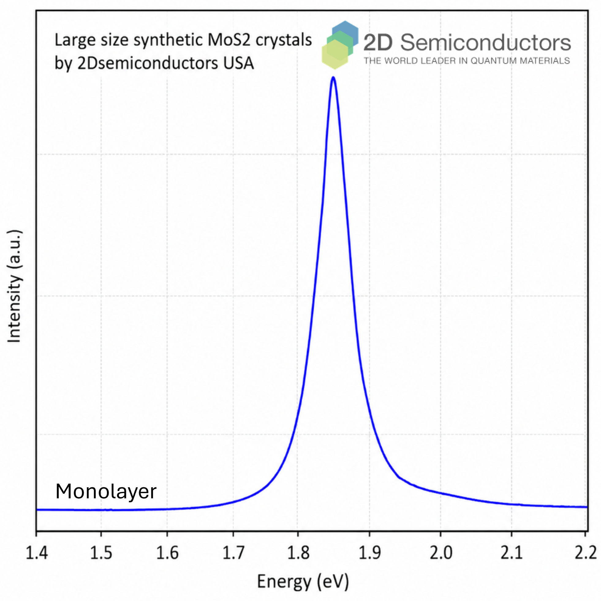
Photoluminescence spectrum (300K) from monolayer Premium MoS2
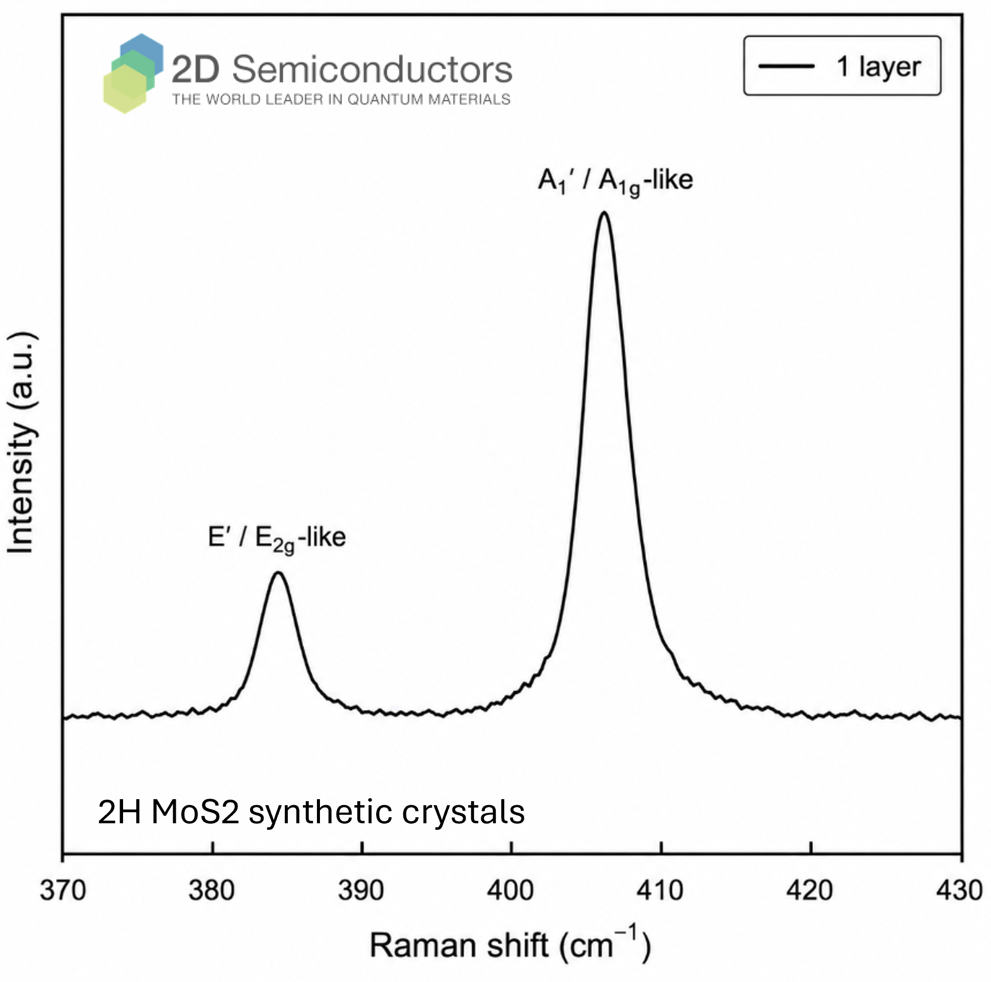
Raman spectrum (300K) from monolayer Premium MoS2 crystals
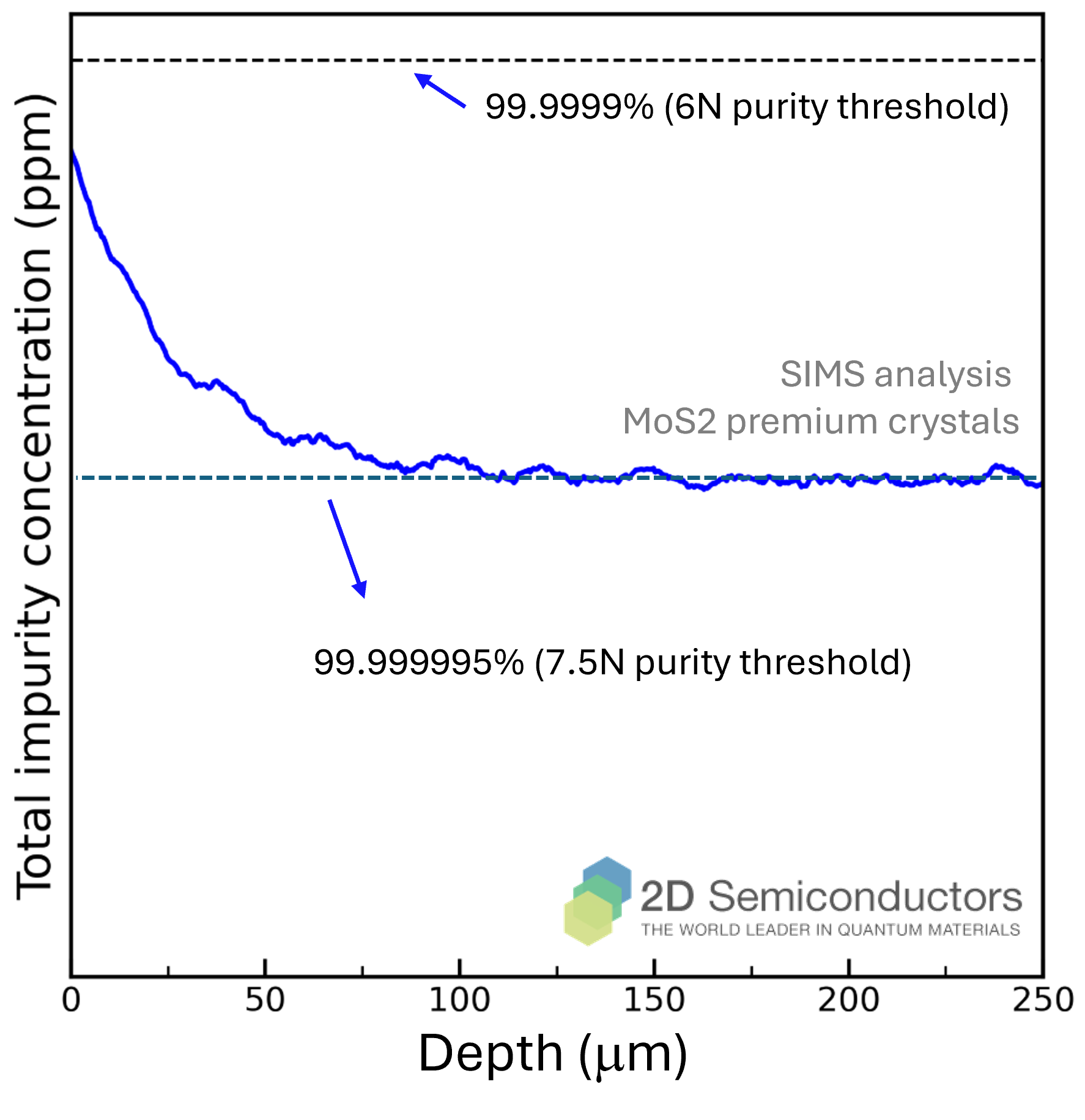
SIMS purity tests from Premium MoS2 crystals
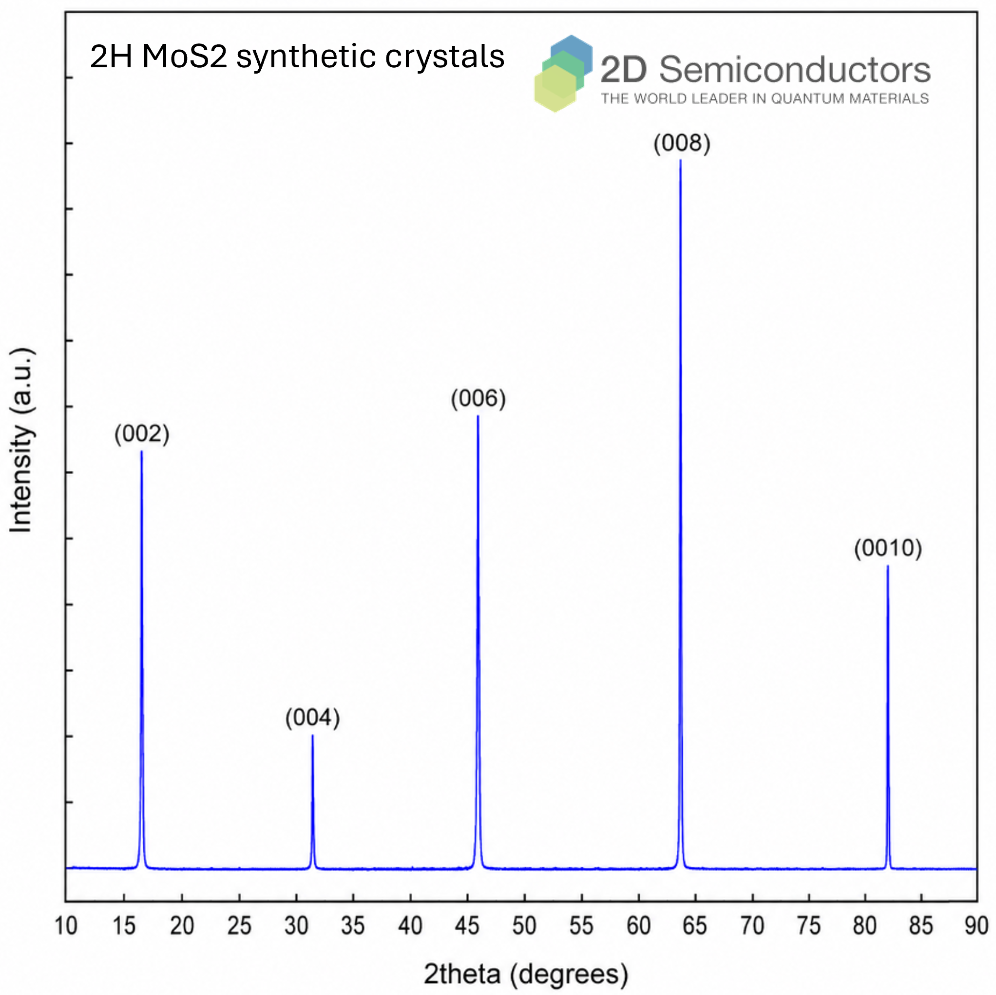
XRD data collected from Premium MoS2 crystals
HRTEM of MoS2 monolayers

Additional Information
Elements: |
Mo,S |
Element: |
Molybdenum |
Element: |
Sulfur |
Formula: |
MoS2 |
Material class: |
MX2 |
Material class: |
Dichalcogen |
Properties: |
Semiconductor |
Properties: |
Excitonic |
Band gap range: |
VIS |
Growth method: |
CVT |
Doping: |
Undoped |
Doping: |
p-Type |
Doping: |
n-Type |
Growth method: |
Flux |
 grown crystals")


