Description
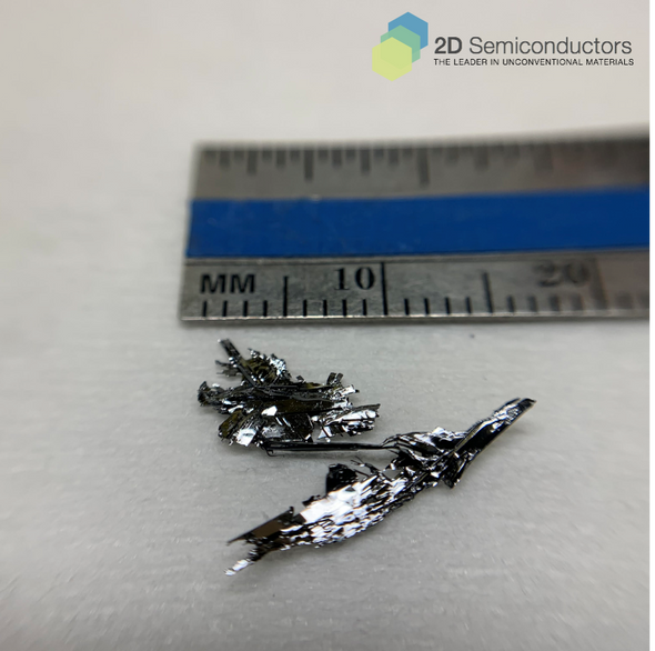
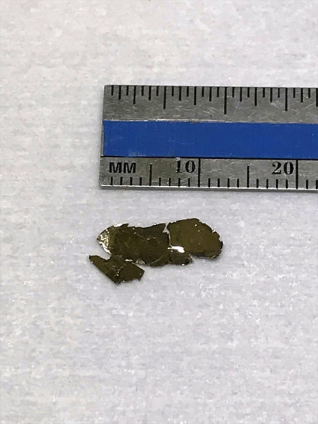
World's largest size commercially available 1T-TaS2 crystals
Our single crystal 1T-phase TaS₂, grown using the superior flux zone technique, guarantees CDW behavior and avoids the contamination issues of chemical vapor transport (CVT). Each growth produces highly crystalline, perfectly oriented (0001) crystals ready for exfoliation. Moreover, these crystals are environmentally stable for long-term use without air interaction concerns.
Flux zone vs. CVT growth method
If you research needs STM grade surfaces or even STM samples (flat crystals mounted on conductive STM holders) please contact us, we will be happy to arrange these samples.
TaS2 characteristics
| Sample size | ~1cm size |
| Material properties | Charge density wave (CDW) material |
| Crystal structure | Hexagonal symmetry |
| Unit cell parameters | a=b=0.335 nm, c=0.593 nm; α=β=90°, γ=120° |
| Growth method | Flux zone (guaranteed no halide contamination) [Optional CVT]: Contains Br2, Cl2, TeCl4, and other halides |
| Purity | 99.9995% confirmed |
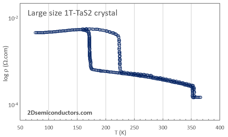
Observed CDW in 1T phase TaS2 crystals from 2Dsemiconductors
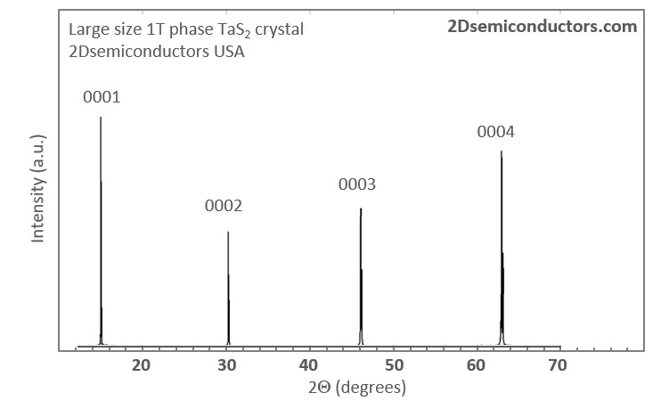
XRD data collected from 1T phase TaS2 crystals
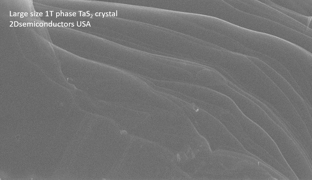
SEM image collected from 1T phase TaS2 crystals
Additional Information
Elements: |
Ta,S |
Element: |
Tantalum |
Element: |
Sulfur |
Formula: |
TaS2 |
Material class: |
MX2 |
Material class: |
Dichalcogen |
Properties: |
Semiconductor |
Properties: |
Semimetal |
Properties: |
CDW |
Band gap range: |
VIS |
Growth method: |
Flux |
Growth method: |
CVT |
Doping: |
Undoped |



![TaS2 [2H-phase] crystals : Large size high quality 2D crystals - 2Dsemiconductors USA TaS2 [2H-phase] crystals : Large size high quality 2D crystals - 2Dsemiconductors USA](https://cdn11.bigcommerce.com/s-i40qayioty/images/stencil/590x590/products/173/979/2H_phase_TaS2_crystals__08973__44251.1704062307.jpg?c=1)
