Description
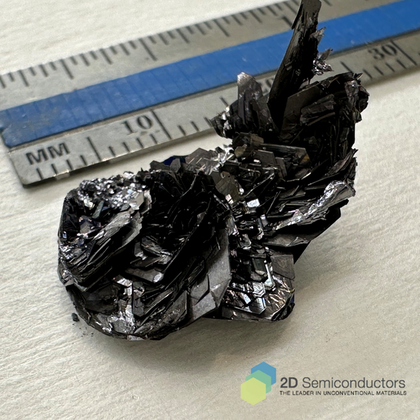
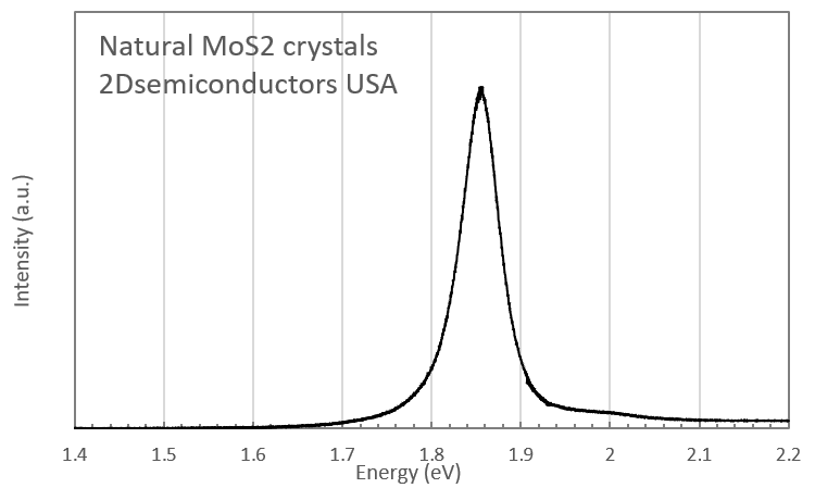
We offer the world’s largest size natural MoS2 crystals, carefully curated for research use. Bulk natural MoS2 is an indirect band gap semiconductor at approximately 1.2 eV and becomes highly luminescent in the monolayer limit with an optical band gap near 1.9 eV.
Compared to our synthetic MoS2, natural crystals are inherently lower in purity and crystallinity and contain higher defect densities. As sourced crystals span a wide size distribution and typically contain significant impurities such as Fe, O, Cr, Ni, C, Se, P, and Si, along with macroscopic defects and cracks.
To ensure research grade quality, each crystal undergoes rigorous multi step cleaning, inspection, and down selection. Impurities are removed from surfaces, edges, and defect rich regions, and structurally compromised areas are discarded. More than 90 percent of the starting material is eliminated, and only the highest quality regions are selected and supplied, not random fragments.
The result is a carefully vetted natural MoS2 crystal optimized for reproducible and high confidence research studies.
Photoluminescence spectrum from monolayer MoS2 sheets exfoliated from MoS2 crystals
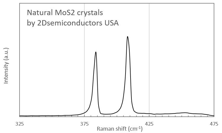
Raman spectrum from synthetic MoS2 crystals
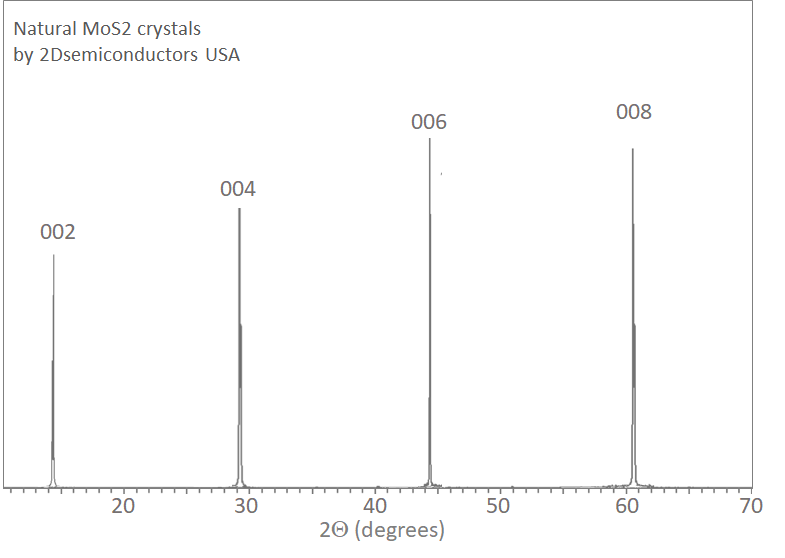
XRD data collected from synthetic MoS2 crystals
Publications from this product
Summary: Publications from Cornell, Washington, MIT, Berkeley, Stanford, and Princeton teams at top journals like Nature, Nature Materials, Nature Communications, Nano Letters, and Advanced Materials
Zefei Wu, Shuigang Xu, Huanhuan Lu, Armin Khamoshi, Gui-Bin Liu, Tianyi Han, Yingying Wu, Jiangxiazi Lin, Gen Long, Yuheng He, Yuan Cai, Yugui Yao, Fan Zhang, and Ning Wang. "Even–odd layer-dependent magnetotransport of high-mobility Q-valley electrons in transition metal disulfides." Nature communications 7, 12955 (2016).
Zefei Wu, Benjamin T. Zhou, Xiangbin Cai, Patrick Cheung, Gui-Bin Liu, Meizhen Huang, Jiangxiazi Lin, Tianyi Han, Liheng An, Yuanwei Wang, Shuigang Xu, Gen Long, Chun Cheng, Kam Tuen Law, Fan Zhang and Ning Wang "Intrinsic valley Hall transport in atomically thin MoS2." Nature communications 10, 611 (2019).
C. Robert, "Optical spectroscopy of excited exciton states in MoS2 monolayers in van der Waals heterostructures" Phys. Rev. Materials 2, 011001(R) (2018)
Weigao Xu et al., "Correlated fluorescence blinking in two-dimensional semiconductor heterostructures", Nature 541, 62-67 (2017), link to article:
http://www.nature.com/nature/journal/v541/n7635/full/nature20601.html
Manish Chhowalla team "Phase-engineered low-resistance contacts for ultrathin MoS2 transistors" Nature Materials DOI: 10.1038/NMAT4080
X. Chen "Probing the electron states and metal-insulator transition mechanisms in molybdenum disulphide vertical heterostructures" Nature Communications 6, Article number: 6088 (2015) doi:10.1038/ncomms7088
Measurement of the optical dielectric function of monolayer transition-metal dichalcogenides: MoS2, MoSe2, WS2, and WSe2, Yilei Li, Alexey Chernikov, Xian Zhang, Albert Rigosi, Heather M. Hill, Arend M. van der Zande, Daniel A. Chenet, En-Min Shih, James Hone, and Tony F. Heinz; Phys. Rev. B 90, 205422 (2014)
H. Wang et.al. "Ultrafast response of monolayer molybdenum disulfide photodetector" Nature Communications 6, Article number: 8831 (2015)
Y. Jin "A Van Der Waals Homojunction: Ideal p–n Diode Behavior in MoSe2" Advanced Materials 27, 5534–5540 (2015)
Tongay et. al. "Defects activated photoluminescence in two-dimensional semiconductors: interplay between bound, charged, and free excitons" Scientific Reports 3, Article number: 2657 (2013)
X Li et al. "Determining layer number of twodimensional flakes of transition-metal dichalcogenides by the Raman intensity from substrates" Nanotechnology 27 (2016) 145704
Tongay et.al. Thermally Driven Crossover from Indirect toward Direct Bandgap in 2D Semiconductors: MoSe2 versus MoS2; Nano Letters, 2012, 12 (11), pp 5576–5580
Manish Chhowalla, "Two-dimensional semiconductors for transistors" Nature Reviews Materials 1, Article number: 16052 (2016) doi:10.1038/natrevmats.2016.52
D. Wolverson et.al. "Raman Spectra of Monolayer, Few-Layer, and Bulk ReSe2: An Anisotropic Layered Semiconductor" ACS Nano, 2014, 8 (11), pp 11154–11164
M. Yankowitz et. al. "Intrinsic Disorder in Graphene on Transition Metal Dichalcogenide Heterostructures" Nano Letters, 2015, 15 (3), pp 1925–1929
H. C. Diaz et.al. "Molecular beam epitaxy of the van der Waals heterostructure MoTe2 on MoS2: phase, thermal, and chemical stability" 2D Materials, Volume 2, Number 4 (2015)
A. Gul et.al. "Theoretical and experimental investigation of conjugation of 1,6-hexanedithiol on MoS2" Materials Research Express, 5 (3), 036415 (2018)
Additional Information
Elements: |
Mo,S |
Element: |
Molybdenum |
Element: |
Sulfur |
Formula: |
MoS2 |
Material class: |
MX2 |
Material class: |
Dichalcogen |
Properties: |
Semiconductor |
Properties: |
Excitonic |
Band gap range: |
VIS |
Growth method: |
Natural |
Doping: |
Undoped |


