 grown crystals")
 grown crystals")


 grown crystals")
 grown crystals")


Description
We guarantee world's largest size commercial crystals with full refund and money back guarantee
We provide 2H-MoS2 synthetic crystals in undoped, p-type, and n-type forms. Our crystals are produced using two methods: Flux zone growth, which offers superior electronic and optical performance, and CVT growth, which provides lower performance but larger sizes (~1,5cm). In contrast, other commercially available 2H-MoS2 crystals are typically derived from natural MoS2 (lowest grade) or CVT growth, which often contains significant contamination from commonly used transport agents.
Our synthetic crystals are among the largest in the world, measuring approximately 1 cm or more. For those requiring 3R-MoS2 crystals for research, please contact us.
For premium ultra flat large size (+2cm) MoS2 crystals follow the link here [Link]
Advantages of our MoS2 crystals
- We offer guaranteed largest size synthetic crystal in the world.
- Only commercially available p-type and n-type MoS2 synthetic crystals
- Confirmed p- and n-type response (excitonic and electronic)
- Excellent customer support and return policy as per US regulations
- 20 years of optimization and perfection in material quality
- Ready to ship across the world.
The properties of MoS2 vdW layered crystals
| Sample size | Larger than 1cm (largest size guaranteed) |
| Material properties | Bulk 1.2 eV indirect and Excitonic semiconductor (~1.85 eV) |
| Crystal structure | 2H semiconducting phase |
| Degree of exfoliation | Easy to exfoliate |
| Production method | Flux zone (higher performance) or CVT (lower performance) |
| Other characteristics |
|
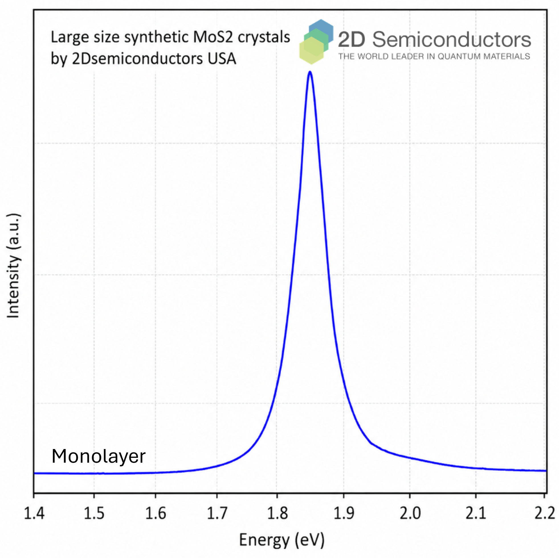
Photoluminescence spectrum from monolayer Premium MoS2
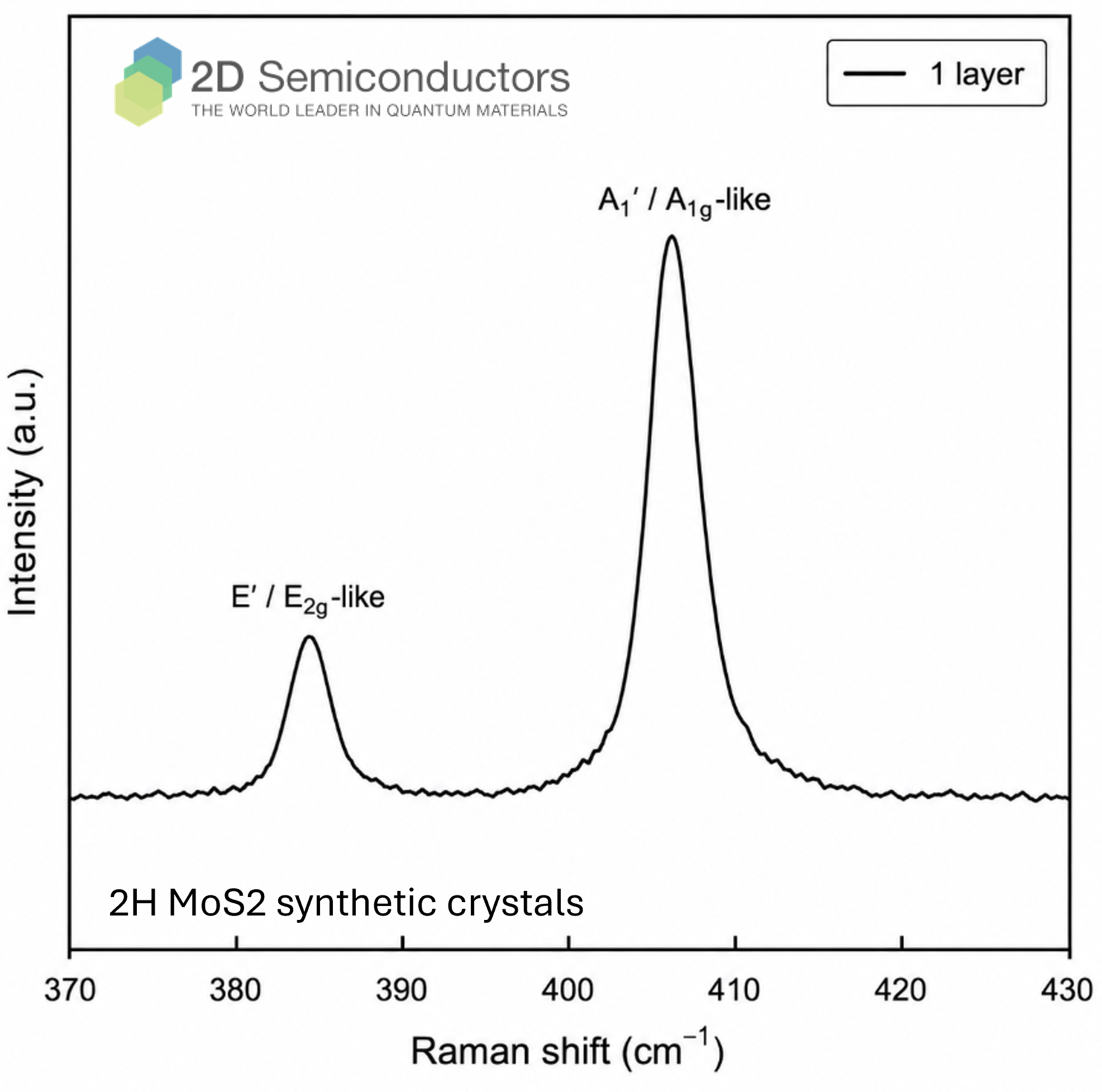
Raman spectrum from monolayer Premium MoS2 crystals
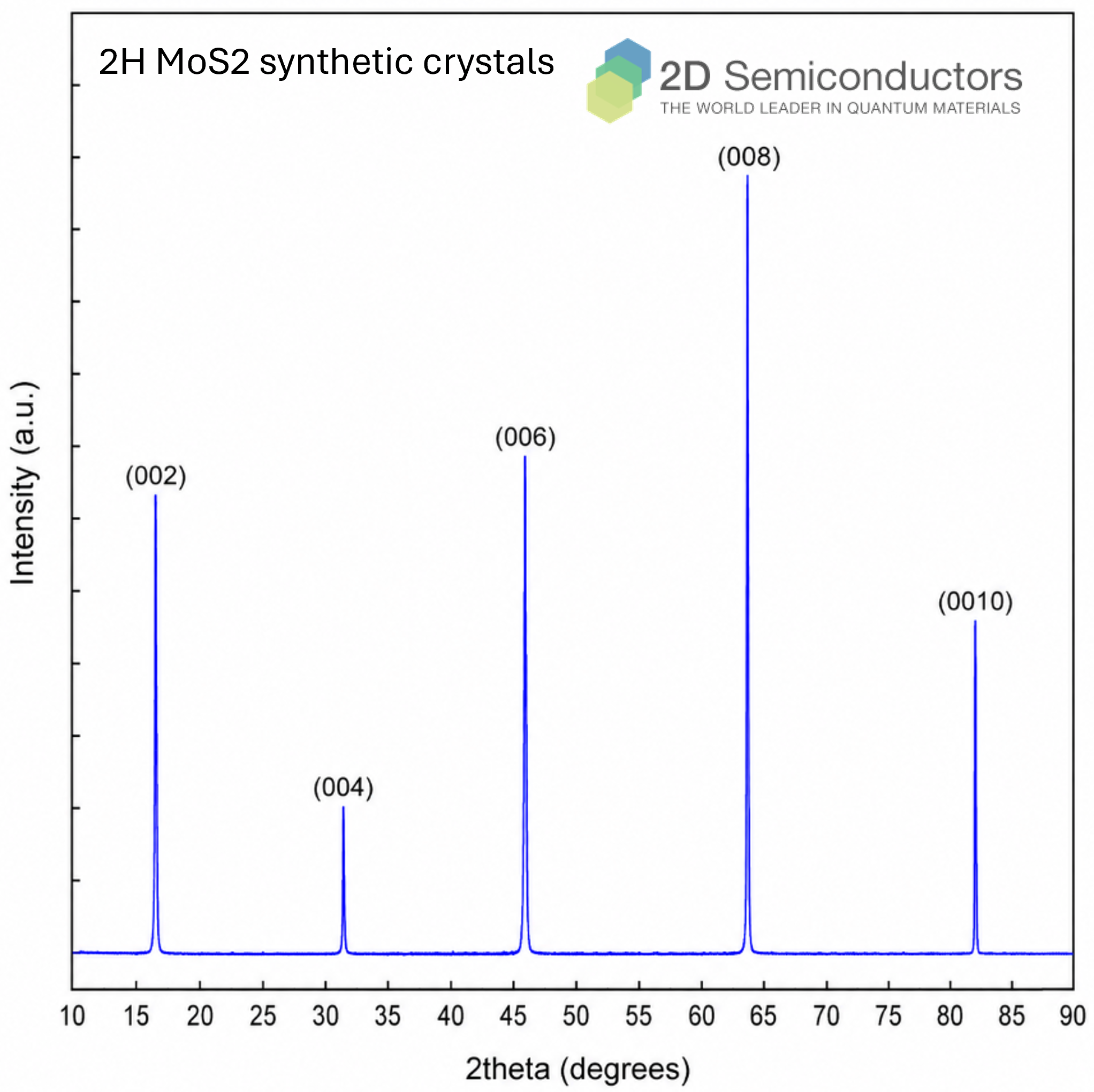
XRD data collected from Premium MoS2 crystals
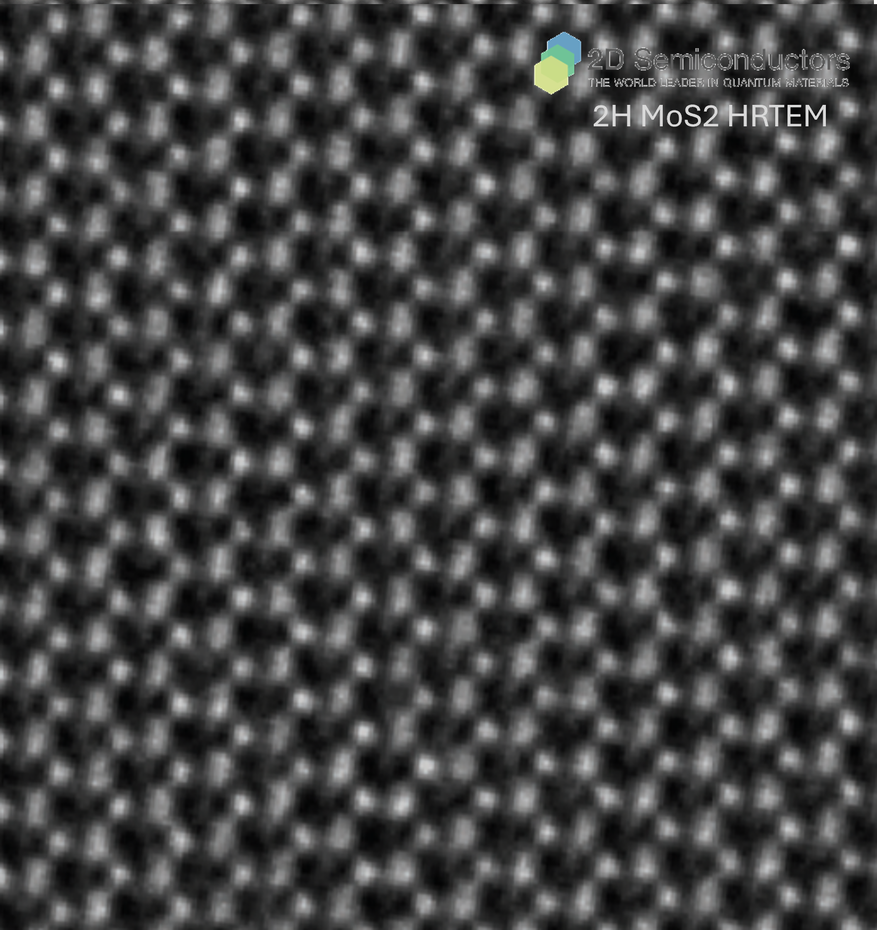
HRTEM of 2H phase MoS2 monolayers
Publications from this product
Summary: Publications from Cornell, Washington, MIT, Berkeley, Stanford, and Princeton teams at top journals like Nature, Nature Materials, Nature Communications, Nano Letters, and Advanced Materials
Negative Differential Photoconductance as a Signature of Nonradiative Energy Transfer in van der Waals Heterojunction
ACS Nano 2021, 15, 10, 16432–16441
Interfacial ferroelectricity in rhombohedral-stacked bilayer transition metal dichalcogenides
Nature Nanotechnology (2022)
Zefei Wu, Shuigang Xu, Huanhuan Lu, Armin Khamoshi, Gui-Bin Liu, Tianyi Han, Yingying Wu, Jiangxiazi Lin, Gen Long, Yuheng He, Yuan Cai, Yugui Yao, Fan Zhang, and Ning Wang. "Even–odd layer-dependent magnetotransport of high-mobility Q-valley electrons in transition metal disulfides." Nature communications 7, 12955 (2016).
Zefei Wu, Benjamin T. Zhou, Xiangbin Cai, Patrick Cheung, Gui-Bin Liu, Meizhen Huang, Jiangxiazi Lin, Tianyi Han, Liheng An, Yuanwei Wang, Shuigang Xu, Gen Long, Chun Cheng, Kam Tuen Law, Fan Zhang and Ning Wang "Intrinsic valley Hall transport in atomically thin MoS2." Nature communications 10, 611 (2019).
C. Robert, "Optical spectroscopy of excited exciton states in MoS2 monolayers in van der Waals heterostructures" Phys. Rev. Materials 2, 011001(R) (2018)
Lu Hua Li et. al. Asymmetric electric field screening in van der Waals heterostructures; Nature Communications 9, 1271 (2018) doi:10.1038/s41467-018-03592-3
X. Wang et.al. "Substrate modified thermal stability of mono- and few-layer MoS2" Nanoscale, 2018, 10, 3540-3546
L. Zhang. et.al. "Photonic-crystal exciton-polaritons in monolayer semiconductors" Nature Communications volume 9, Article number: 713 (2018)
Weigao Xu et al., "Correlated fluorescence blinking in two-dimensional semiconductor heterostructures", Nature 541, 62-67 (2017), link to article:
http://www.nature.com/nature/journal/v541/n7635/full/nature20601.html
Manish Chhowalla team "Phase-engineered low-resistance contacts for ultrathin MoS2 transistors" Nature Materials DOI: 10.1038/NMAT4080
X. Chen "Probing the electron states and metal-insulator transition mechanisms in molybdenum disulphide vertical heterostructures" Nature Communications 6, Article number: 6088 (2015) doi:10.1038/ncomms7088
Measurement of the optical dielectric function of monolayer transition-metal dichalcogenides: MoS2, MoSe2, WS2, and WSe2, Yilei Li, Alexey Chernikov, Xian Zhang, Albert Rigosi, Heather M. Hill, Arend M. van der Zande, Daniel A. Chenet, En-Min Shih, James Hone, and Tony F. Heinz; Phys. Rev. B 90, 205422 (2014)
H. Wang et.al. "Ultrafast response of monolayer molybdenum disulfide photodetector" Nature Communications 6, Article number: 8831 (2015)
Y. Jin "A Van Der Waals Homojunction: Ideal p–n Diode Behavior in MoSe2" Advanced Materials 27, 5534–5540 (2015)
Tongay et. al. "Defects activated photoluminescence in two-dimensional semiconductors: interplay between bound, charged, and free excitons" Scientific Reports 3, Article number: 2657 (2013)
X Li et al. "Determining layer number of twodimensional flakes of transition-metal dichalcogenides by the Raman intensity from substrates" Nanotechnology 27 (2016) 145704
Tongay et.al. Thermally Driven Crossover from Indirect toward Direct Bandgap in 2D Semiconductors: MoSe2 versus MoS2; Nano Letters, 2012, 12 (11), pp 5576–5580
Manish Chhowalla, "Two-dimensional semiconductors for transistors" Nature Reviews Materials 1, Article number: 16052 (2016) doi:10.1038/natrevmats.2016.52
D. Wolverson et.al. "Raman Spectra of Monolayer, Few-Layer, and Bulk ReSe2: An Anisotropic Layered Semiconductor" ACS Nano, 2014, 8 (11), pp 11154–11164
M. Yankowitz et. al. "Intrinsic Disorder in Graphene on Transition Metal Dichalcogenide Heterostructures" Nano Letters, 2015, 15 (3), pp 1925–1929
H. C. Diaz et.al. "Molecular beam epitaxy of the van der Waals heterostructure MoTe2 on MoS2: phase, thermal, and chemical stability" 2D Materials, Volume 2, Number 4 (2015)
A. Gul et.al. "Theoretical and experimental investigation of conjugation of 1,6-hexanedithiol on MoS2" Materials Research Express, 5 (3), 036415 (2018)
C. Robert "Optical spectroscopy of excited exciton states in MoS2 monolayers in van der Waals heterostructures" Phys. Rev. Materials, 2, 011001 (R)
Katharina Greulich; "Charge Transfer from Organic Molecules to Molybdenum Disulfide: Influence of the Fluorination of Iron Phthalocyanine" J. Phys. Chem. C 2020, 124, 31, 16990–16999 (2020)
Additional Information
Elements: |
Mo,S |
Element: |
Molybdenum |
Element: |
Sulfur |
Formula: |
MoS2 |
Material class: |
MX2 |
Material class: |
Dichalcogen |
Properties: |
Semiconductor |
Properties: |
Excitonic |
Band gap range: |
VIS |
Growth method: |
CVT |
Doping: |
Undoped |
Doping: |
p-Type |
Doping: |
n-Type |
Growth method: |
Flux |


