Description
Our MoSSe alloys with the chemical formula MoS2xSe2(1-x) crystals perfectly crystallize in 2H phase and depedning on the composition it can reach to world record ~cm in size. We readily offer x=0, 1/3, 1/2 and 2/3 alloy compositions. MoSSe crystals are grown by flux thus offer superior excitonic and electronic response compared to other commercially available (CVT grown) crystals.
50-50% composition crystals measure around one centimeter or larger in size
Tested more than 100 times, all the crystals come with guaranteed PL spectra, electronic performance, and easy exfoliation characteristics.
Superior performance of our MoSSe crystals
1. No phase separation (no MoS2 or MoSe2 alone inclusions)
2. Confirmed elemental composition
3. Large single domain size and easy exfoliation.
4. Superior performance through flux zone growth
5. Ready to ship.
Properties of layered MoSSe alloys
| Sample size | World record ~cm size |
| Alloying range | x=0 (MoSe2), 1/3, 1/2, 2/3, and 1 (MoS2) |
| Type of alloying | Guaranteed homogenous, no phase separation |
| Properties | 1.56 eV to 1.90 eV (1L MoSe2→1L MoS2) |
| Crystal sturcture | Hexagonal phase |
| Unit cell perameters | Ranges depending on the composition (x) |
| Growth method | [Default] Flux zone (no transport agent contamination) defect free |
| Purity | 99.9999% confirmed |
Growth method matters> Flux zone or CVT growth method? Contamination of halides and point defects in layered crystals are well known cause for their reduced electronic mobility, reduced anisotropic response, poor e-h recombination, low-PL emission, and lower optical absorption. Flux zone technique is a halide free technique used for synthesizing truly semiconductor grade vdW crystals. This method distinguishes itself from chemical vapor transport (CVT) technique in the following regard: CVT is a quick (~2 weeks) growth method but exhibits poor crystalline quality and the defect concentration reaches to 1E11 to 1E12 cm-2 range. In contrast, flux method takes long (~3 months) growth time, but ensures slow crystallization for perfect atomic structuring, and impurity free crystal growth with defect concentration as low as 1E9 - 1E10 cm-2. During check out just state which type of growth process is preferred. Unless otherwise stated, 2Dsemiconductors ships Flux zone crystals as a default choice.
http://meetings.aps.org/Meeting/MAR18/Session/K36.3
http://meetings.aps.org/Meeting/MAR17/Session/V1.14
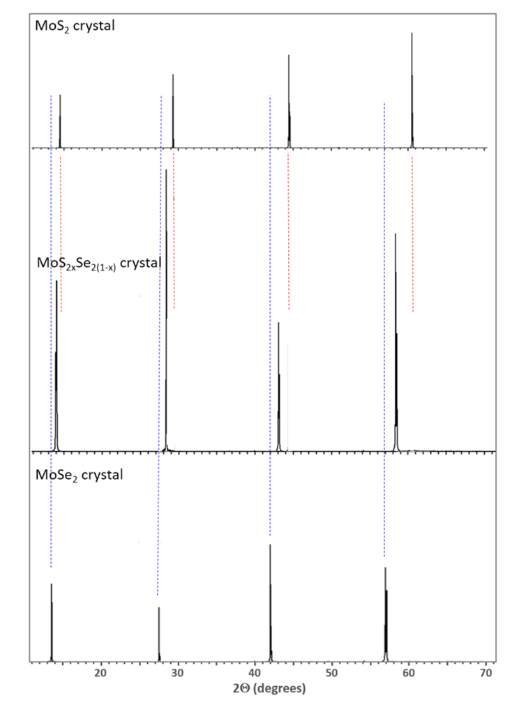
XRD datasets collected from MoSSe alloys

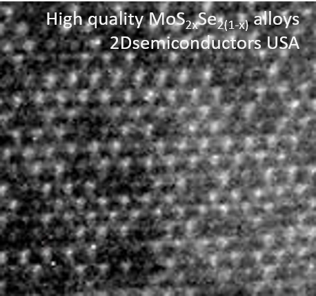
HRTEM image collected from MoSSe crystals

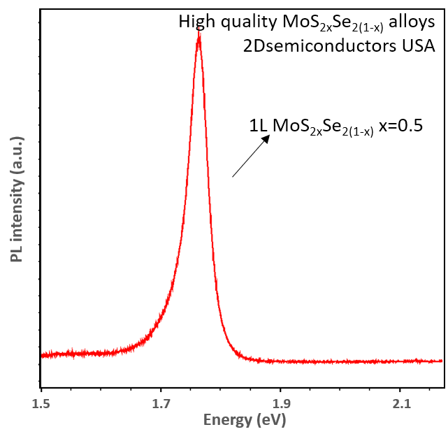
Photoluminescence specturm collected from MoSSe2 at 300K

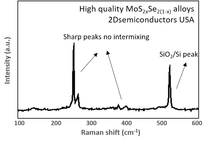
Raman spectrum collected from MoSe2 sheets

Publications from this product
Summary: Publications from MIT, Berkeley, Stanford, Rice, and Harvard teams at top journals like Nature, Nature Communications, Nano Letters, and Advanced Materials
"Chemical Vapor Deposition of High-Optical-Quality Large-Area Monolayer Janus Transition Metal Dichalcogenides" Advanced Materials, 2022
Control of Exciton Valley Coherence in Transition Metal Dichalcogenide Monolayers, Phys. Rev. Lett. 117, 187401 (2016)
Measurement of the optical dielectric function of monolayer transition-metal dichalcogenides: MoS2, MoSe2, WS2, and WSe2, Yilei Li, Alexey Chernikov, Xian Zhang, Albert Rigosi, Heather M. Hill, Arend M. van der Zande, Daniel A. Chenet, En-Min Shih, James Hone, and Tony F. Heinz; Phys. Rev. B 90, 205422 (2014)
Y. Jin "A Van Der Waals Homojunction: Ideal p–n Diode Behavior in MoSe2" Advanced Materials 27, 5534–5540 (2015)
Tongay et. al. "Defects activated photoluminescence in two-dimensional semiconductors: interplay between bound, charged, and free excitons" Scientific Reports 3, Article number: 2657 (2013)
M. Yankowitz et. al. "Intrinsic Disorder in Graphene on Transition Metal Dichalcogenide Heterostructures" Nano Letters, 2015, 15 (3), pp 1925–1929
Tongay et.al. Thermally Driven Crossover from Indirect toward Direct Bandgap in 2D Semiconductors: MoSe2 versus MoS2; Nano Letters, 2012, 12 (11), pp 5576–5580
Manish Chhowalla, "Two-dimensional semiconductors for transistors" Nature Reviews Materials 1, Article number: 16052 (2016) doi:10.1038/natrevmats.2016.52
X Li et al. "Determining layer number of twodimensional flakes of transition-metal dichalcogenides by the Raman intensity from substrates" Nanotechnology 27 (2016) 145704
Additional Information
Elements: |
Mo,S,Se |
Element: |
Molybdenum |
Element: |
Sulfur |
Element: |
Selenium |
Formula: |
MoSSe |
Material class: |
MX2 |
Material class: |
Dichalcogen |
Material class: |
Alloy |
Properties: |
Semiconductor |
Properties: |
Excitonic |
Band gap range: |
VIS |
Growth method: |
Flux |
Growth method: |
CVT |
Doping: |
Undoped |


