Description
Large size WSSe Alloyed Crystals at Designer Concentrations
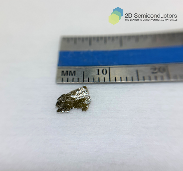
We offer the world's largest size WS2xSe2(1-x) crystals with full money back guarantee: Our WS2xSe2(1–x) alloy crystals (x sulfur concentration) are precision-grown in the stable 2H phase and available at custom alloy ratios x. We use two advanced techniques, chemical vapor transport (CVT) and our modified flux zone growth, to produce phase-pure, homogeneous crystals with exceptional electronic and optical properties. We offer these alloys at designer alloying ratios x. Please indicate your x value during check out.
Product is in stock and ready to ship world wide.
Key Advantages:
-
Uniform Alloying – No phase separation, even at mid-range x values. Each crystal is compositionally consistent across the entire sample.
-
Fully Characterized – XPS, EDS, SAED, PL, XRD, and transport data included with every order.
-
High Optical Quality – Sharp photoluminescence (PL) peaks, narrow linewidths, and low defect density.
-
Electronic-Grade Mobility – Ideal for valleytronics, optoelectronics, and quantum devices.
Backed by over 15 years of R&D, these crystals offer industry-leading purity, stability, and reproducibility. Choose WSSe when performance matters.
Properties of layered WSSe alloys
| Crystal size | ~up to centimeter combined and single size |
| Alloying range | x=0 (WSe2), 0.1, 0.3, 0.5, 0.7, 0.9, 1 (WS2) |
| Type of alloying | Guaranteed homogenous, no phase separation |
| Properties | 1.62 eV to 2.02 eV (1L WSe2→1L WS2) |
| Crystal structure | Hexagonal phase |
| Unit cell parameters | Ranges depending on the composition (x) |
| Growth method | [Default] Flux zone (no halide contamination) defect free [Optional CVT]: Contains Br2, Cl2, TeCl4, and other halides |
| Purity | 99.999% confirmed |
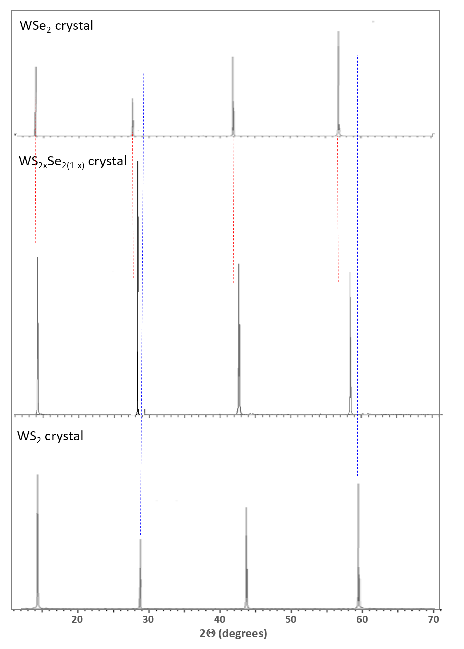
XRD datasets collected from WSSe alloys

Photoluminescence spectrum collected from WSSe2 at 300K

Additional Information
Elements: |
W,S,Se |
Element: |
Tungsten |
Element: |
Sulfur |
Element: |
Selenium |
Formula: |
WSSe |
Material class: |
MX2 |
Material class: |
Dichalcogen |
Material class: |
Alloy |
Properties: |
Semiconductor |
Properties: |
Excitonic |
Band gap range: |
VIS |
Growth method: |
CVT |
Growth method: |
Flux |
Doping: |
Undoped |


