")
")
")
")
")
")
")
")
")
")
")
")
Description
Experience the highest-quality 2H-MoTe2 crystals available anywhere. Our premium flux-grown crystals feature exceptionally flat surfaces, ultra-low defect densities, and world-record crystal sizes ~2 cm. These crystals are specifically optimized for large-area exfoliation and are ideally suited for gold-assisted exfoliation techniques.
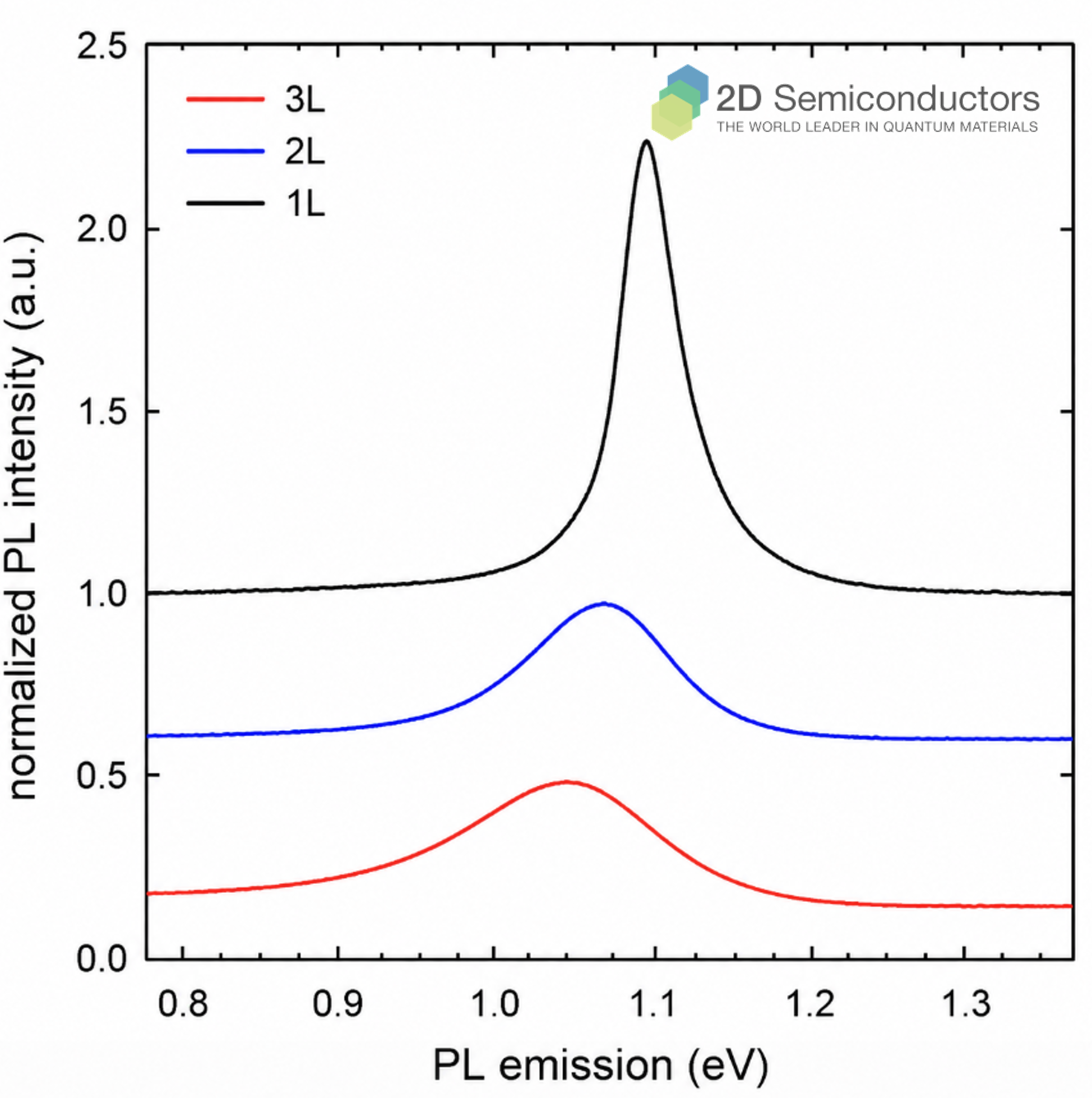
The superior flatness and uniformity enable the isolation of large monolayer and few-layer flakes with excellent yield and reproducibility. With a bulk band gap of approximately 1.0–1.2 eV and a transition toward direct-gap behavior in the monolayer limit, 2H-MoTe2 is a leading material for next-generation electronics, optoelectronics, photodetectors, and excitonic devices.
Characteristics of 2H-MoTe2 crystals from 2Dsemiconductors USA
Materials Project [Link]
C2DB [Link]
| Size | ~2cm size ultra-flat |
| Material properties | 1.2 eV direct gap semiconductors (monolayer) |
| Crystal structure |
Hexagonal phase |
| Unit cell parameters | a=b=0.350 nm, c=1.341 nm; α=β=90° γ=120° |
| Growth method | [Default] Flux zone (no halide contamination) defect free |
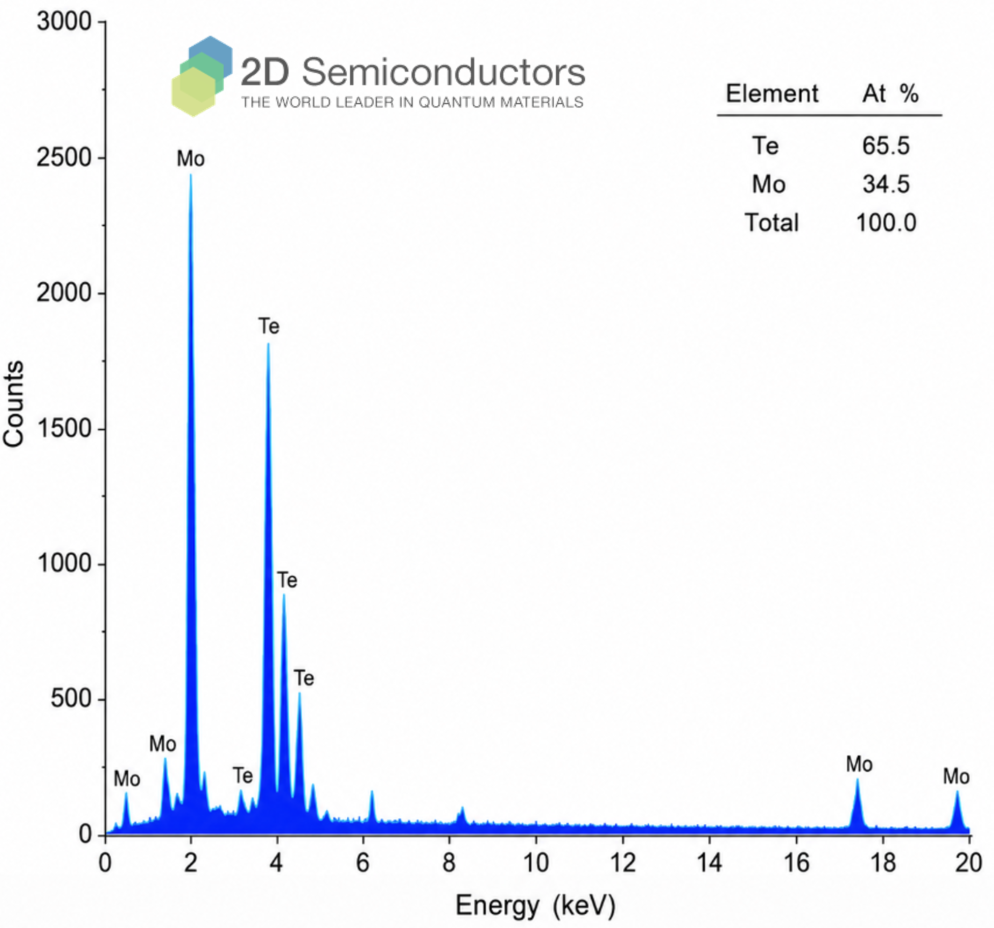
| Purity | 99.9999% confirmed |
| Characteristics |
|
Writing monolithic integrated circuits on a two-dimensional semiconductor with a scanning light probe
Nature Electronics volume 1, pages512–517 (2018)
Y. Li et. al. "Room-temperature continuous-wave lasing from monolayer molybdenum ditelluride integrated with a silicon nanobeam cavity"
Nature Nanotechnology volume 12, pages 987–992 (2017)
Control of Exciton Valley Coherence in Transition Metal Dichalcogenide Monolayers, Phys. Rev. Lett. 117, 187401 (2016)
Tony Heinz Team "Optical Properties and Band Gap of Single- and Few-Layer MoTe2 Crystals" Nano Letters 2014, 14, 6231−6236
Physical origin of Davydov splitting and resonant Raman spectroscopy of Davydov components in multilayer MoTe2; Q. J. Song, Q. H. Tan, X. Zhang, J. B. Wu, B. W. Sheng, Y. Wan, X. Q. Wang, L. Dai, and P. H. Tan; Phys. Rev. B 93, 115409 (2016)
Indirect-to-Direct Band Gap Crossover in Few-Layer MoTe2; Ignacio Gutiérrez Lezama et. al. Nano Letters 2015, 15 (4), pp 2336–2342 DOI: 10.1021/nl5045007
Measurement of the optical dielectric function of monolayer transition-metal dichalcogenides: MoS2, MoSe2, WS2, and WSe2, Yilei Li, Alexey Chernikov, Xian Zhang, Albert Rigosi, Heather M. Hill, Arend M. van der Zande, Daniel A. Chenet, En-Min Shih, James Hone, and Tony F. Heinz; Phys. Rev. B 90, 205422 (2014)
M. Yankowitz et. al. "Intrinsic Disorder in Graphene on Transition Metal Dichalcogenide Heterostructures" Nano Letters, 2015, 15 (3), pp 1925–1929
H. C. Diaz et.al. "Molecular beam epitaxy of the van der Waals heterostructure MoTe2 on MoS2: phase, thermal, and chemical stability" 2D Materials, Volume 2, Number 4 (2015)
S. Vishwanath et. al. "MBE growth of few-layer 2H-MoTe2 on 3D substrates" Journal of Crystal Growth, 482, Pages 61-69 (2018)
Additional Information
Elements: |
Mo,Te |
Element: |
Molybdenum |
Element: |
Tellurium |
Formula: |
MoTe2 |
Material class: |
MX2 |
Material class: |
Dichalcogen |
Properties: |
Semiconductor |
Properties: |
Excitonic |
Band gap range: |
IR |
Growth method: |
Flux |
Growth method: |
CVT |
Doping: |
Undoped |
")
")
")

